Showing posts with label converter. Show all posts
Showing posts with label converter. Show all posts
Monday, October 27, 2014
VGA to BNC Adapter Converter Circuit and explanation
There are monitors which only have three BNC inputs and which use composite synchronization (‘sync on green’). This circuit has been designed with these types of monitor in mind. As can be seen, the circuit has been kept very simple, but it still gives a reasonable performance. The principle of operation is very straightforward. The RGB signals from the VGA connector are fed to three BNC connectors via AC-coupling capacitors. These have been added to stop any direct current from entering the VGA card. A pull-up resistor on the green output provides a DC offset, while a transistor (a BS170 MOSFET) can switch this output to ground. It is possible to get synchronisation problems when the display is extremely bright, with a maximum green component.
In this case the value of R2 should be reduced a little, but this has the side effect that the brightness noticeably decreases and the load on the graphics card increases. To keep the colour balance the same, the resistors for the other two colors (R1 en R3) have to be changed to the same value as R2. An EXOR gate from IC1 (74HC86) combines the separate V-sync and H-sync signals into a composite sync signal. Since the sync in DOS-modes is often inverted compared to the modes commonly used by Windows, the output of IC1a is inverted by IC1b. JP1 can then by used to select the correct operating mode. This jumper can be replaced by a small two-way switch, if required.
This switch should be mounted directly onto the PCB, as any connecting wires will cause a lot of interference. The PCB has been kept as compact as possible, so the circuit can be mounted in a small metal (earthed!) enclosure. With a monitor connected the current consumption will be in the region of 30 mA. A 78L05 voltage regulator provides a stable 5 V, making it possible to use any type of mains adapter, as long as it supplies at least 9 V. Diode D2 provides protection against a reverse polarity. LED D1 indicates when the supply is present. The circuit should be powered up before connecting it to an active VGA output, as otherwise the sync signals will feed the circuit via the internal protection diodes of IC1, which can be noticed by a dimly lit LED. This is something best avoided.
Resistors:
R1,R2,R3 = 470Ω
R4 = 100Ω
R5 = 3kΩ3
Capacitors:
C1,C3,C5 = 47µF 25V radial
C2,C4,C6,C7,C10 = 100nF ceramic
C8 = 4µF7 63V radial
C9 = 100µF 25V radial
Semiconductors:
D1 = LED, high-efficiency
D2 = 1N4002
T1 = BS170
IC1 = 74HC86
IC2 = 78L05
Miscellaneous:
JP1 = 3-way pinheader with jumper
K1 = 15-way VGA socket (female), PCB mount (angled pins)
K2,K3,K4 = BNC socket (female), PCB mount, 75Ω
Read More..
In this case the value of R2 should be reduced a little, but this has the side effect that the brightness noticeably decreases and the load on the graphics card increases. To keep the colour balance the same, the resistors for the other two colors (R1 en R3) have to be changed to the same value as R2. An EXOR gate from IC1 (74HC86) combines the separate V-sync and H-sync signals into a composite sync signal. Since the sync in DOS-modes is often inverted compared to the modes commonly used by Windows, the output of IC1a is inverted by IC1b. JP1 can then by used to select the correct operating mode. This jumper can be replaced by a small two-way switch, if required.
 |  |
 |  |
This switch should be mounted directly onto the PCB, as any connecting wires will cause a lot of interference. The PCB has been kept as compact as possible, so the circuit can be mounted in a small metal (earthed!) enclosure. With a monitor connected the current consumption will be in the region of 30 mA. A 78L05 voltage regulator provides a stable 5 V, making it possible to use any type of mains adapter, as long as it supplies at least 9 V. Diode D2 provides protection against a reverse polarity. LED D1 indicates when the supply is present. The circuit should be powered up before connecting it to an active VGA output, as otherwise the sync signals will feed the circuit via the internal protection diodes of IC1, which can be noticed by a dimly lit LED. This is something best avoided.
Resistors:
R1,R2,R3 = 470Ω
R4 = 100Ω
R5 = 3kΩ3
Capacitors:
C1,C3,C5 = 47µF 25V radial
C2,C4,C6,C7,C10 = 100nF ceramic
C8 = 4µF7 63V radial
C9 = 100µF 25V radial
Semiconductors:
D1 = LED, high-efficiency
D2 = 1N4002
T1 = BS170
IC1 = 74HC86
IC2 = 78L05
Miscellaneous:
JP1 = 3-way pinheader with jumper
K1 = 15-way VGA socket (female), PCB mount (angled pins)
K2,K3,K4 = BNC socket (female), PCB mount, 75Ω

Wednesday, September 10, 2014
Simple Isolated Converter Wiring diagram Schematic
This the Simple Isolated Converter Circuit Diagram. In this Simple Isolated Converter Circuit Diagram a negative output voltage de-de converter generates a -5 V output at pin A. In order to generate -5 Vat point A, the primary of the transformer must fly back to a diode drop more negative than -5 V. If the transformer has a tightly coupled 1/1 turns ratio, there will be a 5 V plus a diode drop across the secondary.
The 1N5817 rectifies this secondary voltage to generate an isolated 5-V output. The isolated output is not fully regulated since only the -5 V at point A is sensed by the MAX635.
Simple Isolated Converter Circuit Diagram
Monday, September 1, 2014
Low Loss Step Down Converter
This schema arose from the need of the author to provide a 5 V output from the 24 V battery of a solar powered genera-tor. Although solar power is essentially free it is important not to be wasteful especially for small installations; if the battery runs flat at midnight you’ve got a long wait before the sun comes up again. The basic requirement was to make an efficient step-down converter to power low voltage equipment; the final design shown here accepts a wide input voltage from 9 to 60 V with an output current of 500 mA. The efficiency is very good even with a load of 1 mA the design is still better than a standard linear regulator. The low quiescent current (200 µA) also plays a part in reducing losses.
Some of the components specified (particularly the power MOSFET) are not the most economical on the market but they have been deliberately selected with efficiency in mind.
Low Loss Step Down Converter Circuit Diagram
When power is applied to the schema a reference voltage is produced on one side of R2. D1 connects this to the sup-ply (pin 7) of IC1 to provide power at start-up. Once the schema begins switching and the output voltage rises to 5 V, D2 becomes forward biased and powers the IC from the output. Diode D1 becomes reverse biased reducing current through R1. When the schema is first powered up the voltage on pin 2 of IC1 is below the reference voltage on pin 3, this produces a high level on output pin 6. The low power MOSFET T1 is switched on which in turn switches the power MOSFET T3 via R5 and the speed-up capacitor C4, the output volt-age starts to rise.
When the output approaches 5 V the voltage fed back to the inverting input of IC1 becomes positive with respect to the non inverting input (reference) and switches the output of IC1 low. T1 and T3 now switch off and C3 transfers this negative going edge to the base of T2 which conducts and effectively shorts out the gate capacitance of T3 thereby improving its switch off time.
The switching frequency is not governed by a fixed clock signal but instead by the load current; with no load attached the schema oscillates at about 40 Hz while at 500 mA it runs at approximately 5 kHz. The variable clock rate dictates that the output inductor L1 needs to have the relatively high value of 100 mH. The coil can be wound on ferrite core material with a high AL value to allow the smallest number of turns and produce the lowest possible resistance. Ready-made coils of this value often have a resistance greater than 1 ? and these would only be suitable for an output load current of less than 100 mA.
The voltage divider ratio formed by R4 and R3 sets the output voltage and these values can be changed if a different out-put voltage is required. The output volt-age must be a minimum of 1 V below the input voltage and the output has a minimum value of 4 V because of the supply to IC1.
A maximum efficiency of around 90 % was achieved with this schema using an input voltage between 9 and 15 V and supplying a current greater than 5 mA, even with an input voltage of 30 V the schema efficiency was around 80 %. If the schema is used with a relatively low input voltage efficiency gains can be made by replacing D4 with a similar device with a lower reverse breakdown voltage rating, these devices tend to have a smaller for-ward voltage drop which reduces losses in the diode at high currents. At higher input voltage levels the value of resistor R1 can be increased proportionally to reduce the quiescent current even further.
Friday, August 29, 2014
Frequency Voltage Converter Wiring diagram Schematic
This is the simple frequency voltage converter schema diagram. Teledyne Semiconductor`s Type TSC9402 is a versatile IC. Not only can it convert voltage into frequency, but also frequency into voltage. It is thus eminently suitable for use in an add-on unit for measuring frequencies with a multimeter.
Only a few additional components are required for this.. Just one calibration point sets the center of the measuring range (or of that part of the range that is used most frequently). The frequency-proportional direct voltage at the output (pin 12—amp out) contains interference pulses at levels up to 0.7 V. If these have an adverse effect on the multimeter, they can be suppressed with the aid of a simple RC network.
The output voltage, U0, is calculated by: tfo=C/rei(Ci + 12 pF) R2fm Because the internal capacitance often has a greater value than the 12 pF taken here, the formula does not yield an absolute value. The schema has a frequency range of dc to 10 kHz. At 10 kHz, the formula gives a value of 3.4 V. The schema draws a current of not more than 1 mA.
Frequency Voltage Converter Circuit Diagram
Simple Frequency Voltage Converter Circuit Diagram
Tuesday, August 12, 2014
Best H E Voltage Converter Wiring diagram Schematic
Best High-efficiency-fly back-voltage-converter. This is a H-E Voltage Converter Circuit Diagram.In this schema Ul is a dual voltage comparator with open collector outputs. The A side is an oscillator operating at 100kHz, and the B side is part of the regulation schema that compares a fraction of the output voltage to a reference generated by zener diode D2.
The output of U1A is applied directly to the gate of Q1. During the positive half-cycle of the Q1 gate voltage, energy is stored in Ll; in the negative half, the energy is discharged into C2. A portion of the output voltage is fed back to U1B to provide regulation. The output voltage is adjustable by changing feedback potentiometer R9.
Best H-E Voltage Converter Circuit Diagram
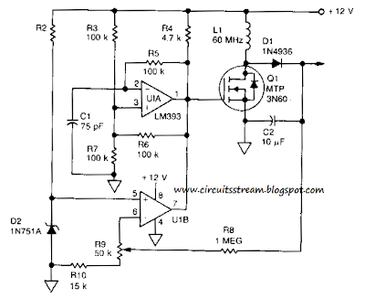
Using the component values shown will produce a nominal 300-V output from a 12-V source. However, the schema maximum output voltage is limited by RlO; a lower value for R10 yields a higher output voltage. The output voltage is also limited by the breakdown of values Ql, L1, D1, and C2.
Saturday, August 9, 2014
Simple Up Controlled Negative Voltage Converter Wiring diagram Schematic
This Simple Up-Controlled Negative Voltage Converter Circuit Diagram was used to produce a variable negative voltage for contrast control of an LCD display. A 74F374 generates a square wave that is ac coupled to a rectifier and load. By using the uP clock and data from the processor bus, and properly timed load signal, the dc level generated can be controlled by the uP.
Simple Up-Controlled Negative Voltage Converter Circuit Diagram

Subscribe to:
Posts (Atom)
