Showing posts with label to. Show all posts
Showing posts with label to. Show all posts
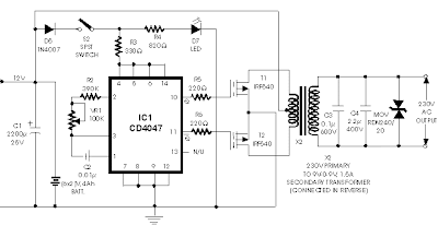
Wednesday, November 12, 2014
Simple 12V DC to 220V 100W Inverter
This is 100W inverter circuit. It uses 4047 IC and IRF540 Mosfet instead of 2N3055 transistor. Power output is 100W from 2-3A transformer.
Sunday, November 2, 2014
LMC7101 LMC7101Q TINY AMPLIFIER WITH RAIL TO RAIL INPUT OUTPUT ELECTRONIC DIAGRAM

LMC7101 - LMC7101Q TINY AMPLIFIER WITH RAIL-TO-RAIL INPUT-OUTPUT ELECTRONIC DIAGRAM
The performance is similar to a single amplifier of the LMC6482/LMC6484 type, with rail-to-rail input and output, high open loop gain, low distortion, and low supply currents. The main benefits of the Tiny package are most apparent in small portable electronic devices, such as mobile phones, pagers, notebook computers, personal digital assistants, and PCMCIA cards.
Monday, October 27, 2014
VGA to BNC Adapter Converter Circuit and explanation
There are monitors which only have three BNC inputs and which use composite synchronization (‘sync on green’). This circuit has been designed with these types of monitor in mind. As can be seen, the circuit has been kept very simple, but it still gives a reasonable performance. The principle of operation is very straightforward. The RGB signals from the VGA connector are fed to three BNC connectors via AC-coupling capacitors. These have been added to stop any direct current from entering the VGA card. A pull-up resistor on the green output provides a DC offset, while a transistor (a BS170 MOSFET) can switch this output to ground. It is possible to get synchronisation problems when the display is extremely bright, with a maximum green component.
In this case the value of R2 should be reduced a little, but this has the side effect that the brightness noticeably decreases and the load on the graphics card increases. To keep the colour balance the same, the resistors for the other two colors (R1 en R3) have to be changed to the same value as R2. An EXOR gate from IC1 (74HC86) combines the separate V-sync and H-sync signals into a composite sync signal. Since the sync in DOS-modes is often inverted compared to the modes commonly used by Windows, the output of IC1a is inverted by IC1b. JP1 can then by used to select the correct operating mode. This jumper can be replaced by a small two-way switch, if required.
This switch should be mounted directly onto the PCB, as any connecting wires will cause a lot of interference. The PCB has been kept as compact as possible, so the circuit can be mounted in a small metal (earthed!) enclosure. With a monitor connected the current consumption will be in the region of 30 mA. A 78L05 voltage regulator provides a stable 5 V, making it possible to use any type of mains adapter, as long as it supplies at least 9 V. Diode D2 provides protection against a reverse polarity. LED D1 indicates when the supply is present. The circuit should be powered up before connecting it to an active VGA output, as otherwise the sync signals will feed the circuit via the internal protection diodes of IC1, which can be noticed by a dimly lit LED. This is something best avoided.
Resistors:
R1,R2,R3 = 470Ω
R4 = 100Ω
R5 = 3kΩ3
Capacitors:
C1,C3,C5 = 47µF 25V radial
C2,C4,C6,C7,C10 = 100nF ceramic
C8 = 4µF7 63V radial
C9 = 100µF 25V radial
Semiconductors:
D1 = LED, high-efficiency
D2 = 1N4002
T1 = BS170
IC1 = 74HC86
IC2 = 78L05
Miscellaneous:
JP1 = 3-way pinheader with jumper
K1 = 15-way VGA socket (female), PCB mount (angled pins)
K2,K3,K4 = BNC socket (female), PCB mount, 75Ω
Read More..
In this case the value of R2 should be reduced a little, but this has the side effect that the brightness noticeably decreases and the load on the graphics card increases. To keep the colour balance the same, the resistors for the other two colors (R1 en R3) have to be changed to the same value as R2. An EXOR gate from IC1 (74HC86) combines the separate V-sync and H-sync signals into a composite sync signal. Since the sync in DOS-modes is often inverted compared to the modes commonly used by Windows, the output of IC1a is inverted by IC1b. JP1 can then by used to select the correct operating mode. This jumper can be replaced by a small two-way switch, if required.
 |  |
 |  |
This switch should be mounted directly onto the PCB, as any connecting wires will cause a lot of interference. The PCB has been kept as compact as possible, so the circuit can be mounted in a small metal (earthed!) enclosure. With a monitor connected the current consumption will be in the region of 30 mA. A 78L05 voltage regulator provides a stable 5 V, making it possible to use any type of mains adapter, as long as it supplies at least 9 V. Diode D2 provides protection against a reverse polarity. LED D1 indicates when the supply is present. The circuit should be powered up before connecting it to an active VGA output, as otherwise the sync signals will feed the circuit via the internal protection diodes of IC1, which can be noticed by a dimly lit LED. This is something best avoided.
Resistors:
R1,R2,R3 = 470Ω
R4 = 100Ω
R5 = 3kΩ3
Capacitors:
C1,C3,C5 = 47µF 25V radial
C2,C4,C6,C7,C10 = 100nF ceramic
C8 = 4µF7 63V radial
C9 = 100µF 25V radial
Semiconductors:
D1 = LED, high-efficiency
D2 = 1N4002
T1 = BS170
IC1 = 74HC86
IC2 = 78L05
Miscellaneous:
JP1 = 3-way pinheader with jumper
K1 = 15-way VGA socket (female), PCB mount (angled pins)
K2,K3,K4 = BNC socket (female), PCB mount, 75Ω
Tuesday, October 14, 2014
MOSFET IRF540 based 100W 12VDC to 220VAC Inverter diagram
The following inverter circuit is using MOSFET transistor IRF540 instead of ordinary transistor (eq 2N3055). FET is better than ordinary transistor in both stability and responsibility.
Thursday, October 2, 2014
How to Make a Simple FM Radio Circuit
This straightforward fm radio receiver circuit involves a regenerative rf stage, TR1, accompanied by a 2 of three-stage sound amplifier, TR2 to TR4.
In certain spots 3 steps of music boosting most likely are not needed, wherein situation TR3 and its related parts could be excluded as well as the free end of capacitor C5 linked to the collector of TR2.
The crucial portion of the fm radio receiver is the initial stage, TR1/VC1, in which the wirings needs to be kept as tight as they can. Coil L1 is established by winding 8 turns of 1mm (20 swg) enamelled copper wire on a six mm diameter former, that may be in that case eliminated. Following that L1 must be extended cautiously and uniformly to a length of about 13mm.
Transistors List
TR1 = BF199
TR2 = TR3 = TR4 = BC547
The tunning capacitor VC1 is among the 2 fm areas of a tiny fm transistor radio with integrated trimmers (VC2). The “earthy” tail (moving vanes and spindle) is hooked up to the 22pF capacitor C1. The value of the rf choke L2 is not important, whatever from 1µH to 10µH genuinely acceptable.
The output is appropriate for regular headphones linked in series to offer an impedance of 64Ω.
Tuning-in the fm radio receiver
To the radio receiver, potentiometer VR1 should initially be promoted gradually (in the direction of the end of the path linked to battery positive) until, at around the half-way position, an abrupt little rise in background disturbances is going to be heard, suggesting the beginning of oscillation. It after that must be assisted off, extremely steadily, until oscillation simply ceases; it next has to be easy to tweak in a few stations.
The right frequency range of 87 MHz to 108 MHz can be acquired by fine-tuning VC2 at the higher frequency (108 MHz) and somewhat flexing or squeezing jointly the turns of coil L1 towards the end (87 MHz).
 About Frequency Modulation
FM transmitting is a transmission know-how pioneered by Edwin Howard Armstrong which employs frequency modulation (FM) to high-fidelity audio over broadcast radio. The "FM band" is the "frequency spectrum wherein FM is utilized for broadcasting". This phrase is moderately inaccurate, because it relates a modulation approach with a variety of frequencies.
In certain spots 3 steps of music boosting most likely are not needed, wherein situation TR3 and its related parts could be excluded as well as the free end of capacitor C5 linked to the collector of TR2.
The crucial portion of the fm radio receiver is the initial stage, TR1/VC1, in which the wirings needs to be kept as tight as they can. Coil L1 is established by winding 8 turns of 1mm (20 swg) enamelled copper wire on a six mm diameter former, that may be in that case eliminated. Following that L1 must be extended cautiously and uniformly to a length of about 13mm.
Transistors List
TR1 = BF199
TR2 = TR3 = TR4 = BC547
The tunning capacitor VC1 is among the 2 fm areas of a tiny fm transistor radio with integrated trimmers (VC2). The “earthy” tail (moving vanes and spindle) is hooked up to the 22pF capacitor C1. The value of the rf choke L2 is not important, whatever from 1µH to 10µH genuinely acceptable.
The output is appropriate for regular headphones linked in series to offer an impedance of 64Ω.
Tuning-in the fm radio receiver
To the radio receiver, potentiometer VR1 should initially be promoted gradually (in the direction of the end of the path linked to battery positive) until, at around the half-way position, an abrupt little rise in background disturbances is going to be heard, suggesting the beginning of oscillation. It after that must be assisted off, extremely steadily, until oscillation simply ceases; it next has to be easy to tweak in a few stations.
The right frequency range of 87 MHz to 108 MHz can be acquired by fine-tuning VC2 at the higher frequency (108 MHz) and somewhat flexing or squeezing jointly the turns of coil L1 towards the end (87 MHz).
FM transmitting is a transmission know-how pioneered by Edwin Howard Armstrong which employs frequency modulation (FM) to high-fidelity audio over broadcast radio. The "FM band" is the "frequency spectrum wherein FM is utilized for broadcasting". This phrase is moderately inaccurate, because it relates a modulation approach with a variety of frequencies.
Thursday, September 4, 2014
How to Reuse Old Cell Battery for LED lighting
Normally cell batteries have a shelf life of 2 to 5 years under normal use. After that time we have to replace them. Nowadays there replacement batteries which are cheap, but these batteries last for much less cost only months. An easy solution is to use batteries in a schema that requires less current, we can use them for lighting LEDs.
How to Reuse Old Cell Battery for LED lighting
![How]()
How to Reuse Old Cell Battery for LED lighting
Saturday, August 30, 2014
Introduction to Amplifier Rise
Amplification is the method of increasing the amplitude of a AC signal current or voltage such as audio signal for sound or video signal for a television picture. The amplifier allows a small input signal to control a bigger amount of power in the output schema. The output signal is a replica of the original input signal but has higher amplitude.
Amplification is necessary as in most applications, the signal is weak to be used directly. For example, an audio output of 1mV from a microphone is unable to drive a loud speaker which requires a few volts to operate. Hence, the signal require to be amplified to a few volts before it can be fed in to the loud speaker.
NP N Transistor Circuit Configurations
An example of different type of transistor configurations in the schema is as shown in Figure one below.

(1) The common emitter(CE) schema makes use of emitter as its common electrode. The input signal is applied to the base and the amplified output is taken from the collector. This is the usually use because its the best combination of current gain & voltage gain.
(2) The common base (CB) schema makes use of base as its common electrode. The input signal is applied to the emitter & the amplified output is taken from the collector. The comparatively high emitter current compared to the base current ends in low input impedance value. For this reason, the CB schema is never used.
(3) The common collector (CC) schema makes use of collector as its common electrode. The input signal is applied to the base & the amplified output is taken from the emitter. This schema is also called an emitter follower. This name means that the output signal voltage at the emitter follows the input signal at the base with the same phase but less amplitude. The voltage gain is less than one & is usually used for impedance matching. Its high input at the base as a load for the earlier schema & low output impedance at the emitter as a signal source for the next schema.
Classes
They can be classified in to classes A, B, C & AB. They are defined based on the percent of the cycle of input signal that can produce output current.
In Class A, the output current flows for the full cycle of 360 degree of input signal. The distortion is the lowest with around 5% to 10% &an efficiency of 20% to 40%. In general, most tiny signal operate class A
In Class C, the output current flows for less than half of the input cycle. Typical operation is 120 degree of input current in the coursework of the positive half cycle of the input current. This class has an efficiency of 80% but has the highest distortion. This class is usually used for RF amplification with a tuned schema in the output.
In Class B, the output current flows for half of the input cycle which is around 180 degree. Class B operation lies between class A & class C. Classes B are usually connected in pairs & in such a schema called push-pull amplifier. The push pull is often used for audio power output to a loud speaker.
In Class AB, it offers a compromise between the low distortion of class A & the higher power of class B. It is usually used for push pull audio power amplifiers.
Wednesday, August 27, 2014
6 to 12 Volt Power Supply Inverter
This inverter circuit can provide up to 800mA of 12V power from a 6V supply. For example, you could run 12V car accessories in a 6V (British?) car. The circuit is simple, about 75% efficient and quite useful. By changing just a few components, you can also modify it for different voltages.
![6]()
Part List:
R1, R4 2.2K 1/4W Resistor
R2, R3 4.7K 1/4W Resistor
R5 1K 1/4W Resistor
R6 1.5K 1/4W Resistor
R7 33K 1/4W Resistor
R8 10K 1/4W Resistor
C1,C2 0.1uF Ceramic Disc Capacitor
C3 470uF 25V Electrolytic Capcitor
D1 1N914 Diode
D2 1N4004 Diode
D3 12V 400mW Zener Diode
Q1, Q2, Q4 BC547 NPN Transistor
Q3 BD679 NPN Transistor
L1 See Notes
MISC Heatsink For Q3, Binding Posts (For Input/Output), Wire, Board
Read More..
Part List:
R1, R4 2.2K 1/4W Resistor
R2, R3 4.7K 1/4W Resistor
R5 1K 1/4W Resistor
R6 1.5K 1/4W Resistor
R7 33K 1/4W Resistor
R8 10K 1/4W Resistor
C1,C2 0.1uF Ceramic Disc Capacitor
C3 470uF 25V Electrolytic Capcitor
D1 1N914 Diode
D2 1N4004 Diode
D3 12V 400mW Zener Diode
Q1, Q2, Q4 BC547 NPN Transistor
Q3 BD679 NPN Transistor
L1 See Notes
MISC Heatsink For Q3, Binding Posts (For Input/Output), Wire, Board
source:LINK
Wednesday, August 20, 2014
Build a Variable 5 to 20V DC Supply Wiring diagram Schematic
This is a Variable 5 to 20V DC Supply Circuit Diagram. If you are looking for a low drop voltage regulator that can provide a power supply of 1A with an output voltage of between 5V and 20V DC, National Semiconductor LM2941 Low Dropout Adjustable Regulator is that you can pick to make use of. Its a typical dropout voltage of 0.5V which means that the input supply need only must be 0.5V DC over the desired output voltage.
Variable 5 to 20V DC Supply Circuit Diagram
Its other features include internal short schema current limit and reverse battery protection. As shown in the schematic below, the regulator has five pins which consists of the ON/OFF control, Input Voltage, Output Voltage, Ground & Adjustable pins. ON/OFF is used for the purpose of switching on & off of the regulator. The capacitors C1 & E1 are to be placed as close as feasible to the regulator.
The output of the schema can be varied by varying the worth of potentiometer VR1 from 5V DC to 20V DC. The input voltage is limited from five.5V DC to 30V DC. Resistor R1 must be greater than 1K. The worth of the VR1 that needs to be set is calculated from the formula given below:
VR1 = R1[(Vout/1.275) - 1] ohm
If R1=1K, Vout = 5V, VR1 should be set to 2.9K ohm.
If R1=1K, Vout = 20V, VR1 should be set to 14.7K ohm

Monday, August 18, 2014
How to Flirt LEDs
A major problem when working with LEDs, is particularly novices connecting the LED to the schema, or how to calculate the value of resistance used. Currently LEDs are very efficient, common and therefore the current needed to illuminate them is quite low: 5mA or less for the LED indicators and 20mA for high brightness LEDs. LEDs are relatively tolerant stream so it can vary between 5mA and 15mA for LED common between 15mA and 30mA for LED high brightness.
The formula for calculating the resistance is obtained by Ohms law and is as follows:
R = (V - V-LED) / I
wherein:
R = resistance
V = voltage
V-LED = LED voltage typical (varies according to whether the LED)
I = current
HI is the current through the LED For example, if we have a red LED connected to 12V with a current of 5mA: R = (12V - 1.2V) / 5mA = 2160 ohms (using default values of resistance: 2.200 ohm)
Calculation base resistors for High Brightness LEDs for voltage 12 Volts
LED Blue and White
Vled v 3.70
current 20mA
Results Resistance: 415 Ohms - 390 Ohms = Approximate
Red LED
Vled v 1.20
current 20mA
Results Resistance: 540 Ohms - 560 Ohms = Approximate
Calculation base resistors for LEDs for normal tension 12 Volts
Red LED
Vled v 1.20
current 5mA
Results Resistance: 2160 Ohms - Approximate = 2k2 Ohms
Green and yellow LED
Vled v 1.60
current 20mA
Results Resistance: 540 Ohms - 560 Ohms = Approximate
Calculation base resistors for High Brightness LEDs for voltage 5 Volts
LED Blue and White
Vled v 3.70
current 20mA
Result of resistance: 65 Ohms - 68 Ohms = Approximate
Red LED
Vled v 1.20
current 20mA
Results Resistance: 190 Ohms - 180 Ohms = Approximate
Calculation base resistors for LEDs to normal voltage 5 Volts
Red LED
Vled v 1.20
current 5mA
Results Resistance: 760 Ohms - 680 Ohms = Approximate
Green and yellow LED
Vled v 1.60
current 20mA
Results Resistance: 680 Ohms - 680 Ohms = Approximate
Take into consideration that there are hundreds of types of LEDs, we just showing the calculation of resistance of LEDs Basic.
There are three types of LEDs:
LED Low current
Typically rated for 2 mA at around 2 V (approximately 4 mW consumption).
LED Standard, Common or Indicator
20 mA LEDs (up to 90 mW) at about:
1.9-2.1 V for the red, orange and yellow,
3.0-3.4 V for green and blue,
2.9 to 4.2 V to violet, pink, purple and white.
High Brightness LED
20 mA at about 2 V or 4-5 V, designed for viewing in direct sunlight.
LED Blue and White
Vled v 3.70
current 20mA
Results Resistance: 415 Ohms - 390 Ohms = Approximate
Red LED
Vled v 1.20
current 20mA
Results Resistance: 540 Ohms - 560 Ohms = Approximate
Calculation base resistors for LEDs for normal tension 12 Volts
Red LED
Vled v 1.20
current 5mA
Results Resistance: 2160 Ohms - Approximate = 2k2 Ohms
Green and yellow LED
Vled v 1.60
current 20mA
Results Resistance: 540 Ohms - 560 Ohms = Approximate
Calculation base resistors for High Brightness LEDs for voltage 5 Volts
LED Blue and White
Vled v 3.70
current 20mA
Result of resistance: 65 Ohms - 68 Ohms = Approximate
Red LED
Vled v 1.20
current 20mA
Results Resistance: 190 Ohms - 180 Ohms = Approximate
Calculation base resistors for LEDs to normal voltage 5 Volts
Red LED
Vled v 1.20
current 5mA
Results Resistance: 760 Ohms - 680 Ohms = Approximate
Green and yellow LED
Vled v 1.60
current 20mA
Results Resistance: 680 Ohms - 680 Ohms = Approximate
Take into consideration that there are hundreds of types of LEDs, we just showing the calculation of resistance of LEDs Basic.
There are three types of LEDs:
LED Low current
Typically rated for 2 mA at around 2 V (approximately 4 mW consumption).
LED Standard, Common or Indicator
20 mA LEDs (up to 90 mW) at about:
1.9-2.1 V for the red, orange and yellow,
3.0-3.4 V for green and blue,
2.9 to 4.2 V to violet, pink, purple and white.
High Brightness LED
20 mA at about 2 V or 4-5 V, designed for viewing in direct sunlight.
Tuesday, August 12, 2014
Mobile phon Circuits to Get Even smaller
Transceivers, appliances such as mobile phones that can send and receive messages, have become smaller and smaller over the last few years, but users are about to experience a new meaning in miniaturisation.
Research at The Hong Kong University of Science & Technology (HKUST) has successfully combined a unique system architecture and new schema design techniques to reduce them in size like never before.
Research at The Hong Kong University of Science & Technology (HKUST) has successfully combined a unique system architecture and new schema design techniques to reduce them in size like never before.
 |
| Transceiver schemary (left) and Dr Leung’s equivalent combining off-chip components |
His research group proposed and demonstrated schema techniques that make it possible to combine many of these components to a single chip and therefore to significantly reduce the size of schemary (see example in graphic). A US patent has been granted for one of the schema techniques.
The transformation applies to the CMOS (Complimentary Metal-Oxide Semiconductor) manufacturing process, which can produce integrated diagram and systems with the highest integration level at the lowest cost. Applying new techniques to the CMOS process, Dr Luong’s research enables many “off-chip” components to be combined to realize a system-on-chip. “But,” he said, “this integration created great challenges in schema implementation.” Part of the research was to solve the problems by new schema design techniques.
“The system architecture and schemary go hand in hand, he added. “They must both work, or neither will be useful.”
The resulting design gives the highest component integration in the smallest chip area ever reported, said Dr Luong.
In his design, all off-chip components are fitted into a central chip measuring 36 mm with packaging, and 8mm without being packaged.
Dr Luong’s miniaturisation method means appliances will soon be made for even lower cost and lower power consumption in addition to being much smaller in size and lighter in weight.
“With the lowering of cost, size and power, many new and interesting applications will become possible and practical,” he said.
Low-power wireless transceivers, for example, could be integrated into implanted devices such as heart pacemakers to wirelessly transmit and receive information between patients and doctors or monitoring systems.
Wearable mobile phones as small as wrist watches at an affordable price could also become a reality.
The transformation applies to the CMOS (Complimentary Metal-Oxide Semiconductor) manufacturing process, which can produce integrated diagram and systems with the highest integration level at the lowest cost. Applying new techniques to the CMOS process, Dr Luong’s research enables many “off-chip” components to be combined to realize a system-on-chip. “But,” he said, “this integration created great challenges in schema implementation.” Part of the research was to solve the problems by new schema design techniques.
“The system architecture and schemary go hand in hand, he added. “They must both work, or neither will be useful.”
The resulting design gives the highest component integration in the smallest chip area ever reported, said Dr Luong.
In his design, all off-chip components are fitted into a central chip measuring 36 mm
Dr Luong’s miniaturisation method means appliances will soon be made for even lower cost and lower power consumption in addition to being much smaller in size and lighter in weight.
“With the lowering of cost, size and power, many new and interesting applications will become possible and practical,” he said.
Low-power wireless transceivers, for example, could be integrated into implanted devices such as heart pacemakers to wirelessly transmit and receive information between patients and doctors or monitoring systems.
Wearable mobile phones as small as wrist watches at an affordable price could also become a reality.
Auther
Principal Investigator
Dr Howard Luong
Subscribe to:
Posts (Atom)
