A circuit for monitoring supply voltages of ±5 V and ±12 V is readily constructed as shown in the diagram. It is appreciably simpler than the usual monitors that use comparators, and AND gates. The circuit is not intended to indicate the level of the inputs. In normal operation, transistors T1 and T3 must be seen as current sources. The drop across resistors R1 and R2 is 6.3 V (12 –5 –0.7). This means that the current is 6.3mA and this flows through diode D1 when all four voltages are present. However, if for instance, the –5 V line fails, transistor T3 remains on but the base-emitter junction of T2 is no longer biased, so that this transistor is cut off. When this happens, there is no current through D which then goes out.
Showing posts with label voltage. Show all posts
Showing posts with label voltage. Show all posts
Thursday, November 6, 2014

Wednesday, November 5, 2014
High Voltage 3 Watt Audio Power Amplifier
The LM4954 is an audio power amplifier primarily designed for demanding applications in mobile phones and other portable communication device applications. It is capable of delivering 2.4 Watts of continuous average power to an 8 BTL load with less than 1% THD+N from a 7VDC power supply. Boomer audio power amplifiers are designed specifically to provide high quality output power with a minimal number of external components. The LM4954 does not require output coupling capacitors or bootstrap capacitors, and therefore is ideally suited for lower-power portable applications where minimal space and power consumption are primary requirements.
BTL load with less than 1% THD+N from a 7VDC power supply. Boomer audio power amplifiers are designed specifically to provide high quality output power with a minimal number of external components. The LM4954 does not require output coupling capacitors or bootstrap capacitors, and therefore is ideally suited for lower-power portable applications where minimal space and power consumption are primary requirements.High Voltage 3 Watt Audio Power Amplifier Circuit Diagram
The LM4954 features a low-power consumption global shutdown mode which is achieved by driving the shutdown pin with logic low. Additionally, the LM4954 features an internal thermal shutdown protection mechanism.
The LM4954 contains advanced pop & click circuitry which eliminates noises that would otherwise occur during turn-on and turn-off transitions.
The LM4954 is unity-gain stable and can be configured by external gain-setting resistors.
Key Specification:
| Wide Power Supply Voltage Range | 2.7 <= VDD <= 9V |
| Output Power: VDD = 7V, 1% THD+N | 2.4W (typ) |
| Quiescent power supply current | 3mA (typ) |
| PSRR: VDD = 5V and 3V at 217Hz | 80dB (typ) |
| Shutdown power supply current | 0.01µA (typ) |
Features:
Wednesday, October 15, 2014
Build a High And Low Voltage Cut Off With Time Delay Circuit Diagrams
The power line fluctuations and cut-offs cause damages to electrical appliances connected to the line. It is more serious in the case of domestic appliances like fridge and air conditioners. If a fridge is operated on low voltage, excessive current flows through the motor, which heats up, and get damaged.
The under/over voltage protection circuit with time delay presented here is a low cost and reliable circuit for protecting such equipments from damages. Whenever the power line is switched on it gets connected to the appliance only after a delay of a fixed time. If there is hi/low fluctuations beyond sets limits the appliance get disconnected. The system tries to connect the power back after the specific time delay, the delay being counted from the time of disconnection. If the power down time (time for which the voltage is beyond limits) is less than the delay time, the power resumes after the delay: If it is equal or more, then the power resumes directly.
This circuit has been designed, built and evaluated by me to use as a protector for my home refrigerator. This is designed around readily available semi-conductor devices such as standard bipolar medium power NPN transistor (D313/SL100/C1061), an 8-pin type 741 op-amp and NE555 timer IC. Its salient feature is that no relay hunting is employed. This draw back is commonly found in the proctors available in the market.
The complete circuit is consisting of various stages. They are: - Dual rail power supply, Reference voltage source, Voltage comparators for hi/low cut offs, Time delay stage and Relay driver stage. Lets now look at the step-by-step design details.
Dual rail power supply.
This is a conventional type of power supply as shown in Figure 1. The power is applied through the step-down transformer (230/12-0-12V/500mA). The DC proportional to the charging input voltage is obtained from bridge rectifier. Two electrolytics are there to bypass any spikes present. Bridge is capable of handling currents up to 1 Amp.
Output is given by: -
V(out) = 0.71 X V (secondary)
= 0.71 X 24V
= 17.04 V
(This equation is similar for the negative rail as well)
This is a conventional type of power supply as shown in Figure 1. The power is applied through the step-down transformer (230/12-0-12V/500mA). The DC proportional to the charging input voltage is obtained from bridge rectifier. Two electrolytics are there to bypass any spikes present. Bridge is capable of handling currents up to 1 Amp.
Output is given by: -
V(out) = 0.71 X V (secondary)
= 0.71 X 24V
= 17.04 V
(This equation is similar for the negative rail as well)
Circuit diagram

Low voltage cut off op-amp
Figure 2 shows the use of very common and easily available op-amp 741 as a comparator. The op-amp is available in TO-5 and DIP type packing.
Figure 2 shows the use of very common and easily available op-amp 741 as a comparator. The op-amp is available in TO-5 and DIP type packing.
Circuit diagram

In this ckt the zener diode D1 and it’s associated resistor R1 are connected to the non-inverting terminal (+ve) of 741 to give the suitable reference voltage. The DC voltage from the sensor is given to the inverting (-ve) terminal through pre-set R2.This is used to set the input level.
When the sensor input is less than Zener voltage the output from the Op-amp remains high and when it is greater than Zener voltage the output goes low. When the sensing voltage is equal to Zener voltage the output of the op-amp is approximately zero.
This phenomenon is used as a decision for switching the relay and to give cutoff in a low voltage situation.
When the sensor input is less than Zener voltage the output from the Op-amp remains high and when it is greater than Zener voltage the output goes low. When the sensing voltage is equal to Zener voltage the output of the op-amp is approximately zero.
This phenomenon is used as a decision for switching the relay and to give cutoff in a low voltage situation.
High voltage cut off op-amp
Here the op-amp is used as a inverted amplifier. See Figure 3.Zener and resistor network gives reference voltage to the inverting terminal (-ve) of op-amp. Sensing voltage derived through the 10 K pre-set is given to the non- inverting (+ve) terminal and this sets the high level cut.
Here the op-amp is used as a inverted amplifier. See Figure 3.Zener and resistor network gives reference voltage to the inverting terminal (-ve) of op-amp. Sensing voltage derived through the 10 K pre-set is given to the non- inverting (+ve) terminal and this sets the high level cut.
When the input DC from the sensor is less than Zener voltage the output of the op-amp is low and vice-versa. When the input DC voltage is equal to the zener voltage, the op-amps output is approximately zero.
Circuit diagram

Time delay
I’ve selected the 555 timer due to following reasons.
1. Timing from microseconds through hours.
2. Ability to operate from wide range of supply voltages.
3. High temperature stability.
4. Easily Available.
5. Its triggering circuit is quite sensitive.
I’ve selected the 555 timer due to following reasons.
1. Timing from microseconds through hours.
2. Ability to operate from wide range of supply voltages.
3. High temperature stability.
4. Easily Available.
5. Its triggering circuit is quite sensitive.
This is basically a monostable. The external timing capacitor C2 is held initially discharged by the timer. The circuit triggers upon receiving a pulse to its pin 2 when the level reaches 1/3 Vcc. Once triggered., the circuit will remain in that state until the set time is elapsed or power to the circuit cuts off. The delayed period in seconds is 1.1 C2.R1 where R1 is in megohms and C2 is in microfarads. In practice, R1 should not exceed 20 M. If you use an electrolytic capacitor for C2, select a unit for low leakage. The time delay may have to be adjusted by varying R1 to compensate for the wide tolerance of electrolytics.
Circuit diagram

Relay Driver
The output from the voltage level detectors cannot directly drive the relay and hence the relay driver is used.
The output from the voltage level detectors cannot directly drive the relay and hence the relay driver is used.
Circuit diagram

In this a relay (12V <500 ohms) is connected to the collector of npn transistor. the out put voltage from the comparator is applied to the base of npn transistor through a resistance r1. when the output from the comparator is low the transistor is in off state and the relay is in de-energized state. similarly when the output from the comparator goes high the transistor switches on and the flow of current from the collector to emitter of transistor energizes the relay.
Generally in a relay driver circuit, parallel to the relay coil, a diode or a capacitor is used. This is to eliminate the back e.m.f generated by the relay coil when currents are suddenly broken. Capacitor C1 is connected in parallel to the coil, which filters out the back emf but it, slows down the working of relay.
A better method is to connect two diodes (as shown in the figure 5) that stop the relay – transistor junction swinging more than 600mV above the positive rail or below the zero-volt rail. During normal operation the diodes are reverse biased and have no effect on the performance of circuit. But when back emf is induced, the diodes conduct heavily and absorb all transient voltages. However, I have employed the both methods.
The Complete Circuit
Circuit diagram

Under normal operating conditions i.e. when the input voltage is between maximum and minimum limit the output from the both the comparators are low. The transistor Q1 is OFF and the relay is in de-energized (pole connected to N/C pin) state and the output is obtained.
When the input voltage is below or above the limits set by the pre-sets R8 or R9, the output of the Op-Amps goes either low or high and diodes D1 or D2 would be forward biased depending on the situation. Transistor Q1 switches ON and the flow of current from collector to emitter energizes the relay and the output is cutoff.
A small amount of hystersis has been added via feed back resistors R10 & R11 so that the relay turns on when the level falls to a particular value but does not turn again until it raises a substantial amount above this value. Other wise the relay contacts will frequently turn on/off and produce chattering.
Construction Hints
1) I used a piece of varoboard, which has copper strips on one side to mount the components, and housed the entire circuit and the transformer in a discarded ATX PC power supply box.
1) I used a piece of varoboard, which has copper strips on one side to mount the components, and housed the entire circuit and the transformer in a discarded ATX PC power supply box.
2) An autotransformer has been used to set the limits. Set the output of the autotransformer to 250V AC and connect it to the primary of transformer T1 (see Figure 1). Then adjust the pre-set R9 such that relay just energizes. This is the high limit. Next set the output of the autotransformer to 200V AC and adjust the pre-set R8 such that the relay energizes. Please note that these are my preferred limits but you may select any range from say 170 to 270V AC.
3) A neon with a suitable resistor could be connected between the AC supply lines as an ON indicator. Alternatively, LED with a current limiting resistor could be connected between the relay coil so when the relay is energized LED will indicate the situation.
Under voltage Indicator for Battery Equipment Circuit Diagram
This is the simple Under voltage Indicator for Battery Equipment Circuit Diagram. Due to the low duty cycle of flashing LED, the average current drain is 1 mA or less. The NE555 will trigger the LED on when the monitored voltage falls to 12 volts.The ratio of Rl to R2 only needs to he changed if it is desired to change the voltage point at which the LED is triggered.
Under voltage Indicator for Battery Equipment Circuit Diagram

Thursday, October 2, 2014
DC High Voltage Protector Circuit Diagram
In case the particular voltage of the mains supply of a computer increases excessive, elements around the printed circuit planks can easily be ruined as well as destroyed.
This kind of unexpected urgent situation cut-out positioned involving the mains supply as well as interrupts the supply if the voltage level exceeds any established value. For a lot of causes its possible for your result voltage of your power supply to increase to some harmful degree. The unexpected urgent situation cut-out described below continues to be arranged towards the highest supply voltage regarding 5.25 V that is explained by the manufacturers associated with TTL ICs.
Zener diode D1 begins doing prior to the particular explained zener voltage is reached. Small current runs in the anode gate circuit of thryristor Th1; the particular level of the current can be arranged with predetermined potentiometer P1 disadvantage connected within side parallel using the door cathode circuit regarding Th1. When the mains supply goes up, the current with the zener diode gets big enough to cause the particular thyristor to fireplace. The actual heating stage lies between 5.2 . . . 6 V. As soon as the thyristor shoots, the principals supply voltage drops substantially because the thyristor practically short-circuits the actual primaries supply. In the case of the supply with out current constraining,merge F1 helps prevent the current will be attaining too high something. The electronic ranking from the blend is dependent, needless to say, about the insert requirement. Throughout screening and also adjusting from the circuit, it is important how the thyristor is constantly on the perform once it has been dismissed till its current provides dropped in order to be able for you to help absolutely no. The particular heating voltage degree may be established by means of a mains supply with a current clipper before it is placed into use.low frequency this shows difficult, because of the tolerances from the zener rectifying tube, to set the shooting voltage for the needed worth, use a 5.1V zener rectifying diode.

This kind of unexpected urgent situation cut-out positioned involving the mains supply as well as interrupts the supply if the voltage level exceeds any established value. For a lot of causes its possible for your result voltage of your power supply to increase to some harmful degree. The unexpected urgent situation cut-out described below continues to be arranged towards the highest supply voltage regarding 5.25 V that is explained by the manufacturers associated with TTL ICs.
Zener diode D1 begins doing prior to the particular explained zener voltage is reached. Small current runs in the anode gate circuit of thryristor Th1; the particular level of the current can be arranged with predetermined potentiometer P1 disadvantage connected within side parallel using the door cathode circuit regarding Th1. When the mains supply goes up, the current with the zener diode gets big enough to cause the particular thyristor to fireplace. The actual heating stage lies between 5.2 . . . 6 V. As soon as the thyristor shoots, the principals supply voltage drops substantially because the thyristor practically short-circuits the actual primaries supply. In the case of the supply with out current constraining,merge F1 helps prevent the current will be attaining too high something. The electronic ranking from the blend is dependent, needless to say, about the insert requirement. Throughout screening and also adjusting from the circuit, it is important how the thyristor is constantly on the perform once it has been dismissed till its current provides dropped in order to be able for you to help absolutely no. The particular heating voltage degree may be established by means of a mains supply with a current clipper before it is placed into use.low frequency this shows difficult, because of the tolerances from the zener rectifying tube, to set the shooting voltage for the needed worth, use a 5.1V zener rectifying diode.
Tuesday, September 9, 2014
Simple Car Battery Voltage Monitor Circuit
A dual op amp is used as a comparator. The green LED on the board, until the voltage exceeds 11.5 volts. The red LED illuminates when the voltage falls below 11.9 volts to the schema. Therefore, in the 11.9 to 11.5 volts, both LEDs are on, producing a slightly yellow color. When the voltage falls below 11.5 V, the green LED, and now only the red LED flashes to indicate low voltage.
Parts List
R1=1K2R2-3-4=680R
R5=15K
R6=10K
R7-8-9-10=1K
IC1=LM324
D1=5V6 /0.5W Zener
D2-3-4-5=LED
RV1=10K trimmer
Is recommended that multi-shaper for V1 and V2. Muti-trimmer makes it much easier to trigger points to make as a less expensive single-turn trimmer. The trimmer can be completely eliminated if you have access to a range of 1% resistors and has had calculated carefully. You would also want to provide more accurate reference voltage as the common 78L05 regulator.
Saturday, September 6, 2014
Monitor voltage and 5VDC and 12VDC Wiring diagram Schematic
This schema is a voltage monitor which operates on fixed testes ± 5 VDC and ± 12 VDC, and is easily constructed as shown in Fig. It is considerably simpler than the normal display using comparators and AND gates. The schema is not intended to indicate the level of entries. If one of the testes fail, for example, -5 V line fails, the transistor Q3 remains on but the base-emitter junction of T2 is not, so that this transistor is cut off. When this happens, there is no current through D, which then turns off.
Monitor voltage + and - 5VDC + and - 12VDC Circuit Diagram
Friday, August 29, 2014
Frequency Voltage Converter Wiring diagram Schematic
This is the simple frequency voltage converter schema diagram. Teledyne Semiconductor`s Type TSC9402 is a versatile IC. Not only can it convert voltage into frequency, but also frequency into voltage. It is thus eminently suitable for use in an add-on unit for measuring frequencies with a multimeter.
Only a few additional components are required for this.. Just one calibration point sets the center of the measuring range (or of that part of the range that is used most frequently). The frequency-proportional direct voltage at the output (pin 12—amp out) contains interference pulses at levels up to 0.7 V. If these have an adverse effect on the multimeter, they can be suppressed with the aid of a simple RC network.
The output voltage, U0, is calculated by: tfo=C/rei(Ci + 12 pF) R2fm Because the internal capacitance often has a greater value than the 12 pF taken here, the formula does not yield an absolute value. The schema has a frequency range of dc to 10 kHz. At 10 kHz, the formula gives a value of 3.4 V. The schema draws a current of not more than 1 mA.
Frequency Voltage Converter Circuit Diagram
Simple Frequency Voltage Converter Circuit Diagram
Thursday, August 14, 2014
Build a High voltage Inverter Wiring diagram Schematic
This is a simple High voltage inverter schema diagram. This inverter schema works with a transistor and transformer and other components to increase the voltage becomes high. Input supply voltage ranging from 3V to 6V DC, later it was raised to high voltage AC. However, in this inverter schema output current is very small, probably under 0.1A even smaller. However, its use you can apply it on a fluorescent lamp 10W maximum power only, and that too takes time to switch on fluorescent lamps.
High voltage inverter schema diagram

Part List
R1 = 4K7
R2 = 2K2
R3 = 330K
C1 = 100nF
C2 = 100nF 275V
C3 = 0.22uF 275V
Q1 = D506
L1 = 100 times winding, with 0.8mm diameter copper wire
L2 = 50 times winding, with 0.8mm diameter copper wire
L3 = 5000 times winding, with 0.4mm diameter copper wire
Tuesday, August 12, 2014
Best H E Voltage Converter Wiring diagram Schematic
Best High-efficiency-fly back-voltage-converter. This is a H-E Voltage Converter Circuit Diagram.In this schema Ul is a dual voltage comparator with open collector outputs. The A side is an oscillator operating at 100kHz, and the B side is part of the regulation schema that compares a fraction of the output voltage to a reference generated by zener diode D2.
The output of U1A is applied directly to the gate of Q1. During the positive half-cycle of the Q1 gate voltage, energy is stored in Ll; in the negative half, the energy is discharged into C2. A portion of the output voltage is fed back to U1B to provide regulation. The output voltage is adjustable by changing feedback potentiometer R9.
Best H-E Voltage Converter Circuit Diagram
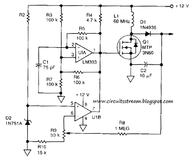
Using the component values shown will produce a nominal 300-V output from a 12-V source. However, the schema maximum output voltage is limited by RlO; a lower value for R10 yields a higher output voltage. The output voltage is also limited by the breakdown of values Ql, L1, D1, and C2.
Battery 9V Voltage Doubler

MAX1044 is a charge pump converter - it uses a capacitor as a "bucket" to pump charge from one place to another. Normally, there is a capacitor connected from pin 2 of the 1044 to pin 4. This capacitor is charged between +9V and ground, and then switched in parallel with a capacitor from pin 5 to ground in a way that makes a negative voltage on the second cap.
In this UPverting use, the 1044 still switches pin 2 between +9V and ground just as it would for a voltage inverter. However, we ignore the pin 4 and 5 connections that would make an inverter from it. Instead, we connect two capacitors and diodes as shown (D1, 2, and C1, 2). The voltage on pin 2 of the 1044 is switched from +9V to ground. When it switches to ground, C1 fills with voltage through D1. When it then switches to +9, it pulls the negative terminal of C1 up to +9V. D1 now blocks any flow of current back into the battery, so the charge in C1 flows through D2 into C2. So at C2, we now get almost 18V!
Theres more. If we add another two diodes and capacitors (D3, D4 and C3, C4), we can add another 9V to it, as C3 charges to +18 through D3 when pin 2 is at ground, and is pulled up to +25 (+27 minus the voltage drops of the diodes) when pin 2 goes high. We can do it again with D5, D6 and C5, C6 to get +33V. The limit on all this is the losses in the diode voltages. Each time we add a section, we add two more diode drops that we cant take advantage of to charge capacitors. But +33 is not bad for a single 9V battery!
If you build this, you MUST take notice of the voltages on the capacitors. The caps can all be the same value, but C1, C2 need to be 25V units, C3, 4, 5, and 6 can be 35V units, and C5 and C6 might need to be 50V unit just for some safety margin. 1N400x diodes work and are cheap, but the losses are higher than they really need to be. For higher performance and lower losses, its better to use something like the 1N5817 schottky diodes for low losses. But both will work.
This charge pumping is a very efficient way to convert voltages. The only power lost is that power dissipated in the resistances of the switches inside the 1044 and the series resistance of the capacitors and diodes, as well as the power to run the internal oscillator that flips the switches when needed.
All by itself, the 1044 runs at about 7-10kHz, so there will be ripple of that amount on the C2 output and on the +9V output from the battery as well. Audio equipment that uses this voltage could have a "whine" audible if youre not careful. However, the 1044 has a frequency boost feature. If you connect pin 1 to the power supply (shown by the little open switch) then the oscillator frequency goes up by about 6:1. The oscillator then works well above the audio region. Any whine is then going to be inaudible.
Sunday, August 10, 2014
Build a Simple 90Vrms Voltage Regulator Circuits Wiring diagram
This is a Simple 90Vrms Voltage Regulator Circuits Diagram. The 90Vrms Voltage Regulator Circuits Diagram is an open loop rms voltage regulator that will provide 500 watts of power at 90 V rms with good regulation for an input voltage range of 110-130 V rms. With the input voltage applied, capacitor Cl charges until the firing point of Q3 is reached causing it to fire.
This turns Q5 on which allows current to flow through the load. As the input voltage increases, the voltage across R10 increases which increases the firing point of Q3. This delays the firing of Q3 because Cl now has to charge to a higher voltage before the peak-point voltage is reached.Thus the output voltage is held fairly constant by delaying the firing of Q5 as the input voltage increases. For a decrease in the input voltage, the reverse occurs.
90Vrms Voltage Regulator Circuits Diagram

Saturday, August 9, 2014
Simple Up Controlled Negative Voltage Converter Wiring diagram Schematic
This Simple Up-Controlled Negative Voltage Converter Circuit Diagram was used to produce a variable negative voltage for contrast control of an LCD display. A 74F374 generates a square wave that is ac coupled to a rectifier and load. By using the uP clock and data from the processor bus, and properly timed load signal, the dc level generated can be controlled by the uP.
Simple Up-Controlled Negative Voltage Converter Circuit Diagram

Network Voltage Indicator Wiring diagram Schematic
Using this schematic is created a network voltage indicator electronic schema. If the input voltage is gift across the network, the optocoupler transistor is open, T1 is blocked and controlled rectifier, Th1, is in a very state of conduction. Since each terminals of the piezoelectric buzzer is at identical potential, buzzer is off. If voltage disappears, the transistor T1 enters the conduction and therefore makes the terminal of buzzer to be placed on the bottom (maintains thyristor conduction state).

during this state of affairs, theres a sufficiently giant potential distinction across the buzzer and D5s to see that these 2 components to point AC power loss, each audible and visual. By pressing the reset button current is interrupted by Th1, therefore thyristor enter in blocking state and therefore the different terminal of the buzzer is connected to ground.
Source by : Streampowers
Friday, August 8, 2014
Supply Voltage Indicator
Supply Voltage Indicator Circuit Diagram. A novel supply voltage monitor which uses a LED to show the status of a power supply.This simple and slightly odd schema can clearly show the level of the supply voltage (in a larger device): as long as the indicator has good 12 volts at its input, LED1 gives steady, uninterrupted (for the naked eye) yellow light. If the input voltage falls below 11 V, LED1 will start to blink and the blinking will just get slower and slower if the voltage drops further - giving very clear and intuitive representation of the supplys status. The blinking will stop and LED1 will finally go out at a little below 9 volts. On the other hand, if the input voltage rises to 13 V, LED2 will start to glow, getting at almost full power at 14 V. The characteristic voltages can be adjusted primarily by adjusting the values of R1 and R4. The base-emitter diode of T2 basically just stands in for a zener diode.

Supply Voltage Indicator Circuit Diagram
The emitter-collector path of T1 is inversely polarized and if the input voltage is high enough - T1 will cause oscillations and the frequency will be proportional to the input voltage. The relaxation oscillator ceases cycling when the input voltage gets so low that it no longer can cause breakdown along the emitter-collector path. Not all small NPN transistors show this kind of behavior when inversely polarized in a similar manner, but many do. BC337-40 can start oscillations at a relatively low voltage, other types generally require a volt or two more. If experimenting, be careful not to punch a hole through the device under test: they oscillate at 9-12 V or not at all.
Subscribe to:
Posts (Atom)
