Showing posts with label diagram. Show all posts

Monday, November 17, 2014

Insect Repeller Circuit Diagram

In this section we talk about a type of insect repellent insect repellent is a circuit that repel insects from your home or garden effectively. This circuit uses the frequency of bullying of insects to the insect goes.

For this insect repellent skesta be installed inside or outside the home can / the speakers. This series of in-circuit PLL oscillator circuit adl / phase looked loop by using a CMOS 4047 at a rate 22 khz.gunakan external power supply for best results.

IC 4047 Description

The CD4047B is capable of operating in either a monostable or astable. It requires an external capacitor (between pins 1 and 3) and an external resistor (between pins 2 and 3) to determine the output pulse width in the monostable mode and the output frequency in astable mode
Absolute Maximum Ratings IC IC 4047

DC Supply Voltage (VDD)...........-0.5V to +18VDC
Input Voltage (VIN)...............-0.5V to VDD +0.5VDC
Storage Temperature Range (TS)....-65°C to +150°C
Power Dissipation (PD)
Dual-In-Line...................... 700 mW
Small Outline..................... 500 mW
Lead Temperature (TL)
(Soldering, 10 seconds)........... 260°C.
Read More..

Thursday, November 13, 2014

Photovoltaic Transimpedance Amplifier Circuit Diagram

Photovoltaic
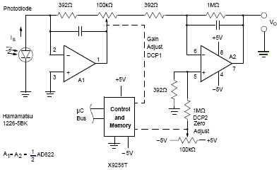
The following schematic shows the Photovoltaic Transimpedance Amplifier Circuit Diagram. This design combines two Intersil X9258T digitally controlled potentiometers with an AD822 low noise dual op amp to create a flexible, digitally calibrated, wide dynamic range transimpedance amplifier topology that can be used with virtually any photovoltaic detector technology. The amplifier output is given by:

Vo = Is(1MΩ) ((1+P1)/(256-P1))

Where P1 is the 8-bit (0 to 255) digital value written to DCP1. For more detail information on Photovoltaic Transimpedance Amplifier Circuit Diagram, download the following file.

Read More..

Tuesday, November 11, 2014

LED flasher with Transistor circuits Diagram

These circuits only flash one or two LEDs. This is opposed to the light chaser circuits that can flash four or more. Of course, the simplest LED flasher is simply to use a flashing LED. The problem with that approach is you have no control over the flash rate, but it does have its use for eye catching displays for selling stuff. The circuits below give you that control, plus they can flash two LEDs alternately.
There are many possible applications for the circuits below, especially for kids, who love flashing lights. Heres some possible uses.
  • Railroad crossing signal for model railroads.
  • Safety blinkers for bicycles, etc.
  • Fun stuff for Halloween, like making those plastic Jack-O-lanterns blink (try using ultraviolet LEDs here).
  • Christmas decorations.
  • Blinkers to locate items in the dark.

Transistor LED flasher

This circuit has a lot going for it. For one thing, it only consists of two transistors, two capacitors and four resistors. That also means it consumes very little power. You can control the flash rate by changing the size of the 100k resistors (100k makes for a pretty slow rate). You can also control the duty cycle by using resistors of different values on the two sides. The 470 ohm resistors control the current through the LEDs. Normally you want to limit this to 20mA, but to conserve battery power, you may need to limit it even further. You can also connect several LEDs in series, instead of using only one for each side. With red LEDs (1 per side) and the values shown, the circuit draws about 11mA. Heres what the actual circuit looks like:


On this circuit, the green wires connect to the LEDs, but you can mount them on the actual circuit board for some applications. The picture is about twice actual size.
Read More..

Monday, November 3, 2014

CHALLENGES DESIGN OF SWITCHING LED ELECTRONIC DIAGRAM


CHALLENGES DESIGN OF SWITCHING LED ELECTRONIC DIAGRAM

The LED WEBENCH® online design environment predicts and simulates the response of an LED to constant current while taking into account several potential design parameters that are new to designers of traditional switching regulators.
Read More..

Sunday, November 2, 2014

LMC7101 LMC7101Q TINY AMPLIFIER WITH RAIL TO RAIL INPUT OUTPUT ELECTRONIC DIAGRAM

LMC7101 - LMC7101Q TINY AMPLIFIER WITH RAIL-TO-RAIL INPUT-OUTPUT ELECTRONIC DIAGRAM

The performance is similar to a single amplifier of the LMC6482/LMC6484 type, with rail-to-rail input and output, high open loop gain, low distortion, and low supply currents. The main benefits of the Tiny package are most apparent in small portable electronic devices, such as mobile phones, pagers, notebook computers, personal digital assistants, and PCMCIA cards.
Read More..

Friday, October 31, 2014

Outdoor Lighting Controller Circuit Diagram

When you step out of your brightly-lit house  into the darkness, it takes a while for your  vision to adjust. A solution to this problem  is this outdoor light with automatic switch-off. As a bonus, it will also make it a little bit  easier to find the keyhole when returning  late at night. Often no mains neutral connection is avail-able at the point where the switch-off timer  is to be installed, which makes many circuit  arrangements impractical. However, the circuit here is designed to work in this situation. The design eschews bulky components such as transformers and the whole unit can  be built into a flush-mounted fitting. The circuit also features low quiescent current consumption.

Outdoor Lighting Controller Circuit Diagram :

Outdoor
The circuit is star ted by closing switch (or  pushbutton) S1. The lamp then immediately receives power via the bridge rectifier. The drop across diodes D5 to D10 is 4.2 V, which provides the power supply for the delay circuit itself, built around the CD4060 binary  counter.

When the switch is opened the lighting sup-ply current continues to flow through Tri1. The NPN optocoupler in the triac drive circuit detects when the triac is active, with antiparallel LED D1 keeping the drive sym-metrical. The NPN phototransistor inside the  coupler creates a reset pulse via T1, driving  pin 12 of the counter. This means that the  full time period will run even if the circuit is retriggered. The CD4060 counts at the AC grid frequency.  Pin 3 goes high after 213clocks, which corresponds to about 2.5 minutes. If this is not long  enough, a further CD4060 counter can be cascaded. T2 then turns on and shorts the internal LED of opto-triac IC2; this causes Tri1 to  be deprived of its trigger current and the light  goes out. The circuit remains without power until next triggered.

The circuit is only suitable for use with resistive loads. With the components shown (in particular in the bridge rectifier and D5 to  D10) the maximum total power of the connected bulb(s) is 200 watts. As is well known, the filament of the bulb is most likely to fail at the moment power is applied. There is little risk to Tri1 at this point as it is bridged by  the switch. The most likely consequence of overload is that one of diodes D1 to D6 will  fail. In the prototype no fuse was used, as it would not in any case have been easy to change. However, that is not necessarily recommended practice!

Circuits at AC line potential should only be constructed by suitably experienced persons and all relevant safety precautions and  applicable regulations must be observed during construction and installation.


Author : Harald Schad - Copyright : Elektor
Read More..

Thursday, October 30, 2014

Project Mini RS232 Data Switch Circuit Diagram

This is the Project of Mini RS232 Data Switch Circuit Diagram. Only simple materials and a little bit of skill are needed to build an RS232 switch. All that you need are two 9-way sub-D plugs with solder pins, a small piece of sheet aluminium, two sets of screw retainer posts, a 4-pole double-throw switch, a strain relief sleeve and a suitable plastic connector shell for a 25-way sub-D connector, with both in-line and right-angle cable entries (such as Conrad Electronics #711322). What is important is that the side cable entry together with its associated strain relief leaves enough room for the switch. If necessary, you may have to cut away a few square millimetres of the sidewall or a few ribs of the plastic shell.

Project image :
 Mini
Mini RS232 Data Switch Image

The switch is operated via the in-line cable opening, as can be seen from the photo. A suitable switch with an overall length of 29 mm can be found in the Conrad catalogue under order number 708232. The only modification that must be made to the connector shell is to drill two holes for the retaining screws for the switch (M2.6 screws) at a spacing of 24 mm.

Mini RS232 Data Switch Circuit diagram :

Mini
Mini RS232 Data Switch Circuit Diagram

Connect the two sub-D connectors together using the piece of aluminium and the screw retainer posts. Then solder the cable to the connectors and the switch as indicated. The two connectors are wired somewhat differently. While the upper sub-D plug is connected 1:1 with the input cable (with the switch in the appropriate position), the DCD, DTR, DSR and RI pins of the lower connector are left open. This is because RTS and CTS are fully sufficient for handshaking, as long as DTR and DSR are connected to each other. The only leads that are switched are RXD, RTS, TSD and CTS. The ground potential is fed from the cable to both connectors. After everything has been properly soldered together, you can fit everything into the cable shell as shown.
Read More..

On Demand WC Fan Using 555 Circuit Diagram

In most WCs with an extractor the fan is connected to the lighting circuit and is switched on and off either in sympathy with the light or with a short delay. Since toilets are sometimes used for washing the hands or just for a quick look in the mirror, it is not always necessary to change the air in the smallest room in the house. The following circuit automatically determines whether there really is any need to run the fan and reacts appropriately. No odour sensor is needed: we just employ a small contact that detects when and for how long the toilet seat lid is lifted.

On-Demand WC Fan circuit Using 555

On-Demand

If the seat lid is left up for at least some presettable minimum time t1, the fan is set running for another presettable time t2. In the example shown the contact is made using a small magnet on the lid and a reed switch mounted on the cistern. The rest is straightforward: IC2, the familiar 555, forms a timer whose period can be adjusted up to approximately 10 to 12 minutes using P2. This determines the fan running time. There are three CMOS NAND gates (type 4093) between the reed switch and the timer input which generate the required trigger signal. When the lid is in the ‘up’ position the reed switch is closed.

Capacitor C1 charges through P1 until it reaches the point where the output of IC1a switches from logic 1 to logic 0. The output of IC1b then goes to logic 1. The edge of the 0-1 transition, passed through the RC network formed by C2 and R2, results in the output of IC1c going to logic 0 for a second. This is taken to the trigger input on pin 2 of timer IC2, which in turn switches on the relay which causes the fan to run for the period of time determined by P2. The circuit is powered from a small transformer with a secondary winding delivering between approximately 8 V and 10 V. Do not forget to include a suitable fuse on the primary side.

The circuit around IC1b and IC1c ensures that the fan does not run continuously if the toilet seat lid is left up for an extended period. The time constant of P1 and C1 is set so that the fan does not run as a result of lavatorial transactions of a more minor nature, where the lid is opened and then closed shortly afterwards, before C1 has a chance to charge sufficiently to trigger the circuit.
Read More..

Wednesday, October 29, 2014

Fog Lamp Sensor Circuit Diagram

Here are simple Fog Lamp Sensor Circuit Diagram. For several years now, a rear fog lamp has been mandatory for trailers and caravans in order to improve visibility under foggy conditions.

Circuit diagram :
Fog Lamp Sensor Circuit Diagram

When this fog lamp is switched on, the fog lamp of the pulling vehicle must be switched off to avoid irritating reflections. For this purpose, a mechanical switch is now built into the 13-way female connector in order to switch off the fog lamp of the pulling vehicle and switch on the fog lamp of the trailer or caravan. For anyone who uses a 7-way connector, this switching can also be implemented electronically with the aid of the circuit illustrated here.

Here a type P521 optocoupler detects whether the fog lamp of the caravan or trailer is connected. If the fog lamp is switched on in the car, a current flows through the caravan fog lamp via diodes D1 and D2. This causes the LED in the optocoupler to light up, with the result that the phototransistor conducts and energises the relay via transistor T1. The relay switches off the fog lamp of the car.

For anyone who’s not all thumbs, this small circuit can easily be built on a small piece of perforated circuit board and then fitted somewhere close to the rear lamp fitting of the pulling vehicle.


Author :Harrie Dogge - Copyright : Elektor
Read More..

Triangle Square Wave Oscillator Circuit Diagram

By making Rt variable it is possible to alter the operating frequency over a 100 to 1 range. Versatile triangle/squarenvave oscillator has a possible frequency range of 0 Hz to 100 kHz.


Simple Triangle Square Wave Oscillator Circuit Diagram


Simple

Read More..

Friday, October 17, 2014

25W Audio Power Amplifier Circuits Diagram

This audio power amplifier project is based on LM1875 amplifier module from National Semiconductor. It can deliver up to 30W of power using an 8 ohm load & dual 30V DC power supplies. It is designed to operate with maximum outside parts with current limit & thermal shutdown protection features . Other features include high gain, quick slew rate, wide power supply range, giant output voltage swing & high current capability.

Summary of the audio amply-fire features:

  • Low distortion: 0.015%, 1 kHz, 20 W
  • Wide power bandwidth: 70 kHz
  • Wide supply range 16V-60V
  • Up to 30 watts output power
  • Internal output protection diodes
  • Protection for AC & DC short circuits to ground
  • 94 dB ripple rejection
  • Plastic power package TO-220
25V Power Supply

The schematic below shows how the +25V DC & -25V DC are obtained. In order to provide power supply for two stereo amplifiers, a power transformer rating of 80VA with 240V/36V middle tapped secondary winding is used. The secondary output of the transformer is rectified by using 1N5401 diodes together with four electrolytic capacitors to smoother the ripple voltage. A fuse & a varistor are connected at the primary input to protect the circuit against power surge.

25W


Audio Amplifier Module

The +25V & -25V DC power supply are connected to the audio amplifier module through a 2A fuse with the peripheral devices shown in the schematic below. The audio input signal to be amplified is coupled to pin one of LM1875 through the resistor R1 and electrolytic capacitor E5.

The output signal at pin four of LM1875 can be used to directly drive a 8 ohm loudspeaker. Resistor R6 and capacitor C5 prevent-the capacitance developed at the long speaker leads from driving the amplifier in to High Frequency Oscillation.

A heat-sink with a thermal resistance rating of one.4 Cecilius/Watt or better must be used or else the amplifier module will-be cut-off from operation due to the heat that will build up in the coursework of the operation of the amplifier. Take note that the heat sink tab on the IC module is internally connected to the -25V power supply hence it must be isolated from the heat sink by the use of an insulating washer. If this is not done, the negative rail will be shorted to ground.

25W


Read More..

Wednesday, October 15, 2014

Build a 70 Watt OCL Amplifier Circuit Diagram

OCL power amplifier circuit used in the circuit above is the type of power amplifier OCL (Output Capacitor Less) with a power output of 70 Watt. Circuit 70 Watt power amplifier OCL is working on a class AB with symmetrical voltage source of VCC ± 25 volts DC to ± 32 volts DC. OCL power amplifier circuit uses a 70 watt power transistor complementary transistor TIP in 2955 and TIP 3055. 70 watt power amplifier in the circuit can be used to drive the load (4-16 Ohm loudspeaker). Power supply circuit power amplifier can use power supply circuit with current 5A symmetrical. For stereo audio system needs to make a power amplifier OCL circuit tone control + over 2 units.

70 Watt OCL Amplifier Circuit Diagram


Read More..

Under voltage Indicator for Battery Equipment Circuit Diagram

This is the simple Under voltage Indicator for Battery Equipment Circuit Diagram. Due to the low duty cycle of flashing LED, the average current drain is 1 mA or less. The NE555 will trigger the LED on when the monitored voltage falls to 12 volts.The ratio of Rl to R2 only needs to he changed if it is desired to change the voltage point at which the LED is triggered.


Under voltage Indicator for Battery Equipment Circuit Diagram

Under

Read More..

Sunday, October 5, 2014

Low Cost Universal Charger Circuit Diagram


Here is the ambit diagram of a low amount accepted charger for NiCD - NiMH batteries. This ambit is Ideal for car use. It has adeptness to transform a mains adapter in to a charger . This one can be acclimated to allegation cellular phone, toys, portables, video batteries, MP3 players, ... and has selectable allegation current. An LED is amid in ambit to announce charging. Can be congenital on a accepted purpose PCB or a veroboard. I achievement you absolutely like it.

Low Cost Universal Charger Circuit Diagram Prt

R1 = 120R-0...5W
R2 = See Diagram
C1 = 220uF-35V
D1 = 1N4007
D2 = 3mm. LED
Q1 = BD135
J1 = DC Input Socket
Read More..

Saturday, October 4, 2014

Telephone line monitor Circuit Diagram

TelephoneTelephone line monitor Circuit Diagram

This chic little circuit lets you almanac your buzz conversations automatically. The accessory connects to the buzz line, your band recorders microphone input, and the recorders alien ascendancy jack. It senses the voltage in the buzz band and begins recording back the band drops to 5 volts or less.

Parts
R1 270K 1/4 W Resistor
R2 1.5K 1/4 W Resistor
R3 68K 1/4 W Resistor
R4 33K 1/4 W Resistor
C1 0.22uF 150 Volt Capacitor
Q1, Q2 2N4954 NPN Transistor
D1 1N645 Diode
MISC Wire, Plugs To Match Jacks On Recorder, Board, Phone Plug

Notes
1. The circuit can be placed anywhere on the phone line, even inside a phone.
2. Some countries or states require you to notify anyone you are talking to that the conversation is being recorded. Most recoders do this with a beep-beep. Also, you may have to get permission from the phone company before you connect anything to their lines.

Read More..

Thursday, October 2, 2014

DC High Voltage Protector Circuit Diagram

In case the particular voltage of the mains supply of a computer increases excessive, elements around the printed circuit planks can easily be ruined as well as destroyed.
This kind of unexpected urgent situation cut-out positioned involving the mains supply as well as interrupts the supply if the voltage level exceeds any established value. For a lot of causes its possible for your result voltage of your power supply to increase to some harmful degree. The unexpected urgent situation cut-out described below continues to be arranged towards the highest supply voltage regarding 5.25 V that is explained by the manufacturers associated with TTL ICs.
Zener diode D1 begins doing prior to the particular explained zener voltage is reached. Small current runs in the anode gate circuit of thryristor Th1; the particular level of the current can be arranged with predetermined potentiometer P1 disadvantage connected within side parallel using the door cathode circuit regarding Th1. When the mains supply goes up, the current with the zener diode gets big enough to cause the particular thyristor to fireplace. The actual heating stage lies between 5.2 . . . 6 V. As soon as the thyristor shoots, the principals supply voltage drops substantially because the thyristor practically short-circuits the actual primaries supply. In the case of the supply with out current constraining,merge F1 helps prevent the current will be attaining too high something. The electronic ranking from the blend is dependent, needless to say, about the insert requirement. Throughout screening and also adjusting from the circuit, it is important how the thyristor is constantly on the perform once it has been dismissed till its current provides dropped in order to be able for you to help absolutely no. The particular heating voltage degree may be established by means of a mains supply with a current clipper before it is placed into use.low frequency this shows difficult, because of the tolerances from the zener rectifying tube, to set the shooting voltage for the needed worth, use a 5.1V zener rectifying diode.


Read More..

Saturday, September 20, 2014

Explanation Fuse Box Chevrolet Corsica 1992 Diagram

Fuse Box Chevrolet Corsica 1992 Diagram - This show you about Fuse Box Chevrolet Corsica 1992 Diagram.

Fuse Box Chevrolet Corsica 1992 Diagram


Fuse
Fuse

Fuse Panel Layout Diagram Parts: fuel injector, stop light, hazard light, radio, air bag, ignition coil, stop light, alternator, anti lock brake, back up light, turn signal lamp, trunk release, cigar lighter, parking light, side marked light, license light, heater, air conditioner, warning indicator, rear window defogger, windshield wiper/washer, trunk release, radio CD, power window, rear window defogger, autoatic door unlock.
Read More..

Fuse Box BMW Z3 Roadster 1998 Diagram

Fuse Box BMW Z3 Roadster 1998 Diagram - Here are new post for Fuse Box BMW Z3 Roadster 1998 Diagram.

Fuse Box BMW Z3 Roadster 1998 Diagram


Fuse
Fuse

Fuse Panel Layout Diagram Parts: auxiliary fuse box,. high beam light relay, crash control module, fuel pump relay.
Read More..

Fuse Box Toyota 1999 Corolla CE Diagram

Fuse Box Toyota 1999 Corolla CE Diagram - Here are new post for Fuse Box Toyota 1999 Corolla CE Diagram.

Fuse Box Toyota 1999 Corolla CE Diagram


Fuse
Fuse

Fuse Panel Layout Diagram Parts: window defogger, power window, noise filter, taillight control relay, integration relay, turn fuse, gauge fuse, wiper, ECU ignition fuse, stop lamp fuse, taillight fuse, door fuse, steering fuse, cigar lighter.
Read More..

Friday, September 19, 2014

Hot Fox Hunt Transmitter Circuit Diagram

http://www.open-circuit.co.uk/pic/tro2dia.gif


If the U1 output is “0″, transistor T3 is off and the transmitter is also off. On the other hand, if the U1 output is “1″, transistor T3 is on and the transmitter is on. During the “1″ period, gate U2 generates a square wave signal with a frequency form 0.1 to 1Hz. Gate U3 works as an inverter only. It determines whether gate U4 generates a 1KHz signal or not. A periodic burst signal is now present at the gate FET T2 to modulate the transmitter used at foxhunt.

Calibration of the foxhunt transmitter: Adjust the three trimmer capacitors to produse a maximum signal amplitude at the output.

Coil Data:
L1 = 470 nH
L2 is made of 5 windings of 0.8mm copper wire, 8 mm winding diameter. It is tapped at the first winding from the ground.

L3 is made of 0.8mm copper wire, 8mm winding diameter, 3 windings at the FET side and 2 windings at the antenna side. Adjust the coupling between the two windings sides to get a maximum signal output amplitude.
The circuit can be powered with a 9 volt battery. It consumes around 20mA only.

Fox Hunt Transmitter Active Components.

T1 = 2SA256
T2 = 3N205
U1, U2, U3, U4 = IC1 = 4093
Read More..