Thursday, November 13, 2014
Latest Step Up Booster Powers Eight White LEDs Diagram Circuit
The constant-current design of the circuit guarantees a steady current through all LEDs, regardless of the forward voltage differences between them. Although this circuit was designed to operate from a single Li-Ion battery (2.5V to 4.5V), the LT1615 is also capable of operating from inputs as low as 1 V with relevant output power reductions. The Motorola MBR0520 surface mount Schottky diode (0.5 A 20 V) is a good choice for D1 if the output voltage does not exceed 20 V. In this application however, it is better to use a diode that can withstand higher voltages like the MBR0540 (0.5 A, 40 V). Schottky diodes, with their low forward voltage drop and fast switching speed, are the best match.
Many different manufacturers make equivalent parts, but make sure that the component is rated to handle at least 0.35 A. Inductor L1, a 4.7-µH choke, is available from Murata, Sumida, Coilcraft, etc. In order to maintain the constant off-time (0.4 ms) control scheme of the LT1615, the on-chip power switch is turned off only after the 350-mA (or 100-mA for the LT1615-1) current limit is reached. There is a 100-ns delay between the time when the current limit is reached and when the switch actually turns off. During this delay, the inductor current exceeds the current limit by a small amount. This current overshoot can be beneficial as it helps increase the amount of available output current for smaller inductor values.

This will be the peak current passed by the inductor (and the diode) during normal operation. Although it is internally current-limited to 350 mA, the power switch of the LT1615 can handle larger currents without problems, but the overall efficiency will suffer. Best results will be o btained when IPEAK is kept well below 700 mA for the LT1615.The LT1615 uses a constant off-time control scheme to provide high efficiencies over a wide range of output current. The LT1615 also contains circuitry to provide protection during start-up and under short-circuit conditions.
When the FB pin voltage is at less than approximately 600 mV, the switch off-time is increased to 1.5 ms and the current limit is reduced to around 250 mA (i.e., 70% of its normal value). This reduces the average inductor current and helps minimize the power dissipation in the LT1615 power switch and in the external inductor L1 and diode D1. The output current is determined by Vref/R1, in this case, 1.23V/68 = 18 mA). Further information on the LT1615 may be found in the device datasheets which may be downloaded from www.linear-tech.com/pdf/16151fa.pdf
Copyright: Elektor Electronics

Wednesday, November 12, 2014
PWM Discrete Generator Circuit and explanation
Discrete PWM Generator Circuit Diagram
An extension of the circuit shown can produce two PWM wave-forms from an 8-bit digital input word. Each signal has 15 values. The 8-bit word can be produced for example from an expansion board fitted in a PC or from an 8-bit port of a processor which does not have built-in PWM capability or from a laptop’s printer port. The mark/space ratio is only programmable up to 15/16 rather than 16/16; a binary input of 0000 produces a continuous low on both outputs turning both motors off.
Similar circuits often employ a dedicated ‘enable’ input to turn the motors off but it is not necessary in this design. The diagram shows the circuitry required to produce just one waveform. For the full two channel circuit it is necessary to use an additional 74HC193. The clock signal produced by the HCF4060 generator can be used to drive both channels and the free flip flop in the 74HC74 package can be used for the second channel (the corresponding pin numbers are shown in brackets). Altogether the entire two channel circuit can be built using just four ICs.
Monday, October 27, 2014
TDA2030 bridge 35 watt power amplifier Diagram Circuit
A very simple 35 watt power amplifier electronic project can be designed using the TDA2030 power audio IC. The TDA2030A is a monolithic IC in Pentawatt package intended for use as low frequency class AB amplifier.
The TDA2030A provides high output current and has very low harmonic and cross-over distortion. TDA2030 ICs connected in bridge mode.
This circuit require few external electronics parts and supports a 8 ohms load . This 35 watt power amplifier require a very good filtered DC power supply , that will provide an output voltage of +/- 16 volts .
Using this circuit you can design a very simple and efficiency subwoofer amplifier with a maximum output power of 35 watt power .
The device incorporates a short circuit protection system comprising an arrangement for automatically limiting the dissipated power so as to keep the working point of the output transistors within their safe operating area. Also a conventional thermal shut-down system is also included .
However a heatsink must be used for the TDA2030 bridge circuit but for any reason, if the junction temperature increases up to 150oC, the thermal shut-down simply reduces the power dissipation and the current consumption.
LM4765 2 x 30 watt amplifier Diagram Circuit
A very simple 2 x 30 watt amplifier electronic circuit project can be designed using the LM4765 stereo audio amplifier IC capable of delivering typically 30W per channel of continuous average output power into an 8Ω load with less than 0.1% THD+N.
This 2 x 30 watt amplifier electronic circuit is very simple and require few external electronic parts and can be used in high end stereo TVs or some other audio applications .
Each amplifier has an independent smooth transition fadein/out mute and a power conserving standby mode which can be controlled by external logic.
Like many other audio amplifier ICs the LM4765 has many features like Temperature protection circuitry, SPiKe protection ( means that these parts are safeguarded at the output against overvoltage, undervoltage, overloads, including thermal runaway and instantaneous temperature peaks).
This audio amplifier electronic circuit project can be powered from a wide input voltage range from 20 volt up to 66 volts , but typically is required a dual 28 volts input ( take care because |Vcc|+|Vee|<60 volts .
The audio IC must be mounted on a heat sink to keep the die temperature at a level such that the thermal protection circuitry does not operate under normal circumstances.
In this circuit diagram is represented just a part of the IC (one channel ) and numbers in parentheses represent pinout for amplifier B
VGA to BNC Adapter Converter Circuit and explanation
In this case the value of R2 should be reduced a little, but this has the side effect that the brightness noticeably decreases and the load on the graphics card increases. To keep the colour balance the same, the resistors for the other two colors (R1 en R3) have to be changed to the same value as R2. An EXOR gate from IC1 (74HC86) combines the separate V-sync and H-sync signals into a composite sync signal. Since the sync in DOS-modes is often inverted compared to the modes commonly used by Windows, the output of IC1a is inverted by IC1b. JP1 can then by used to select the correct operating mode. This jumper can be replaced by a small two-way switch, if required.
 |  |
 |  |
This switch should be mounted directly onto the PCB, as any connecting wires will cause a lot of interference. The PCB has been kept as compact as possible, so the circuit can be mounted in a small metal (earthed!) enclosure. With a monitor connected the current consumption will be in the region of 30 mA. A 78L05 voltage regulator provides a stable 5 V, making it possible to use any type of mains adapter, as long as it supplies at least 9 V. Diode D2 provides protection against a reverse polarity. LED D1 indicates when the supply is present. The circuit should be powered up before connecting it to an active VGA output, as otherwise the sync signals will feed the circuit via the internal protection diodes of IC1, which can be noticed by a dimly lit LED. This is something best avoided.
Resistors:
R1,R2,R3 = 470Ω
R4 = 100Ω
R5 = 3kΩ3
Capacitors:
C1,C3,C5 = 47µF 25V radial
C2,C4,C6,C7,C10 = 100nF ceramic
C8 = 4µF7 63V radial
C9 = 100µF 25V radial
Semiconductors:
D1 = LED, high-efficiency
D2 = 1N4002
T1 = BS170
IC1 = 74HC86
IC2 = 78L05
Miscellaneous:
JP1 = 3-way pinheader with jumper
K1 = 15-way VGA socket (female), PCB mount (angled pins)
K2,K3,K4 = BNC socket (female), PCB mount, 75Ω
Saturday, October 25, 2014
Energy Saver Relay Coil Diagram Circuit
Circuit diagram:
The action of C2 causes the full supply voltage to appear briefly across the relay coil, which helps to activate the relay as fast as possible. Via T2, a delay network consisting of C1 and R2 controls the relay coil current flowing through T1 and R3, effectively reducing it to half the ‘pull in’ current. Diode D2 discharges C1 when the control voltage is Low. Around one second will be needed to completely discharge C1. T2 shunts the bias current of T1 when the delay has elapsed. Diode D1 helps to discharge C1 as quickly as possible. The relay shown in the circuit was specified at 12 V / 400 ohms. All component values for guidance only.
Tuesday, October 14, 2014
MOSFET IRF540 based 100W 12VDC to 220VAC Inverter diagram
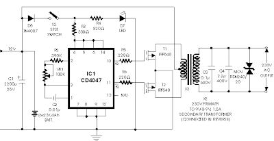
The following inverter circuit is using MOSFET transistor IRF540 instead of ordinary transistor (eq 2N3055). FET is better than ordinary transistor in both stability and responsibility.
Monday, October 13, 2014
STA575 200 watt stereo power audio amplifier circuit
STA575 power audio amplifier can be set in three states by the Stby/mute pin: Standby ( Vpin <0.8v), mute (1.6v
In the Standby mode all the circuits involved in the signal path are in off condition, instead in Mute mode the circuits are biased but the Speakers Outputs are forced to ground potential.
These voltages can be get by the external RC network connected to Stby/Mute pin.
The same block is used to force quickly the I.C. In standby mode or in mute mode when the I.C. dangerous condition has been detected.
The protection of STA575 power audio amplifier are implemented by the Over Temperature, Unbalance .
The Output bridge amplifier makes the single-ended to Differential conversion of the Audio signal using two power amplifiers, one in non-inverting configuration with gain equal to 2 and the other in inverting configuration with unity gain.
To power this 200 watt stereo power audio amplifier you’ll need a DC power source that will provide the following output voltages : Vs+ = 28V, Vs- = -23V, VCD+ = 20V, VCD- = -20V and you’ll need a 8 ohms load .
In the table bellow you can see values for electronic parts required by this 200 watt stereo power audio amplifier electronic project .
