Showing posts with label low. Show all posts
Showing posts with label low. Show all posts
Wednesday, October 15, 2014
Build a High And Low Voltage Cut Off With Time Delay Circuit Diagrams
The power line fluctuations and cut-offs cause damages to electrical appliances connected to the line. It is more serious in the case of domestic appliances like fridge and air conditioners. If a fridge is operated on low voltage, excessive current flows through the motor, which heats up, and get damaged.
The under/over voltage protection circuit with time delay presented here is a low cost and reliable circuit for protecting such equipments from damages. Whenever the power line is switched on it gets connected to the appliance only after a delay of a fixed time. If there is hi/low fluctuations beyond sets limits the appliance get disconnected. The system tries to connect the power back after the specific time delay, the delay being counted from the time of disconnection. If the power down time (time for which the voltage is beyond limits) is less than the delay time, the power resumes after the delay: If it is equal or more, then the power resumes directly.
This circuit has been designed, built and evaluated by me to use as a protector for my home refrigerator. This is designed around readily available semi-conductor devices such as standard bipolar medium power NPN transistor (D313/SL100/C1061), an 8-pin type 741 op-amp and NE555 timer IC. Its salient feature is that no relay hunting is employed. This draw back is commonly found in the proctors available in the market.
The complete circuit is consisting of various stages. They are: - Dual rail power supply, Reference voltage source, Voltage comparators for hi/low cut offs, Time delay stage and Relay driver stage. Lets now look at the step-by-step design details.
Dual rail power supply.
This is a conventional type of power supply as shown in Figure 1. The power is applied through the step-down transformer (230/12-0-12V/500mA). The DC proportional to the charging input voltage is obtained from bridge rectifier. Two electrolytics are there to bypass any spikes present. Bridge is capable of handling currents up to 1 Amp.
Output is given by: -
V(out) = 0.71 X V (secondary)
= 0.71 X 24V
= 17.04 V
(This equation is similar for the negative rail as well)
This is a conventional type of power supply as shown in Figure 1. The power is applied through the step-down transformer (230/12-0-12V/500mA). The DC proportional to the charging input voltage is obtained from bridge rectifier. Two electrolytics are there to bypass any spikes present. Bridge is capable of handling currents up to 1 Amp.
Output is given by: -
V(out) = 0.71 X V (secondary)
= 0.71 X 24V
= 17.04 V
(This equation is similar for the negative rail as well)
Circuit diagram

Low voltage cut off op-amp
Figure 2 shows the use of very common and easily available op-amp 741 as a comparator. The op-amp is available in TO-5 and DIP type packing.
Figure 2 shows the use of very common and easily available op-amp 741 as a comparator. The op-amp is available in TO-5 and DIP type packing.
Circuit diagram

In this ckt the zener diode D1 and it’s associated resistor R1 are connected to the non-inverting terminal (+ve) of 741 to give the suitable reference voltage. The DC voltage from the sensor is given to the inverting (-ve) terminal through pre-set R2.This is used to set the input level.
When the sensor input is less than Zener voltage the output from the Op-amp remains high and when it is greater than Zener voltage the output goes low. When the sensing voltage is equal to Zener voltage the output of the op-amp is approximately zero.
This phenomenon is used as a decision for switching the relay and to give cutoff in a low voltage situation.
When the sensor input is less than Zener voltage the output from the Op-amp remains high and when it is greater than Zener voltage the output goes low. When the sensing voltage is equal to Zener voltage the output of the op-amp is approximately zero.
This phenomenon is used as a decision for switching the relay and to give cutoff in a low voltage situation.
High voltage cut off op-amp
Here the op-amp is used as a inverted amplifier. See Figure 3.Zener and resistor network gives reference voltage to the inverting terminal (-ve) of op-amp. Sensing voltage derived through the 10 K pre-set is given to the non- inverting (+ve) terminal and this sets the high level cut.
Here the op-amp is used as a inverted amplifier. See Figure 3.Zener and resistor network gives reference voltage to the inverting terminal (-ve) of op-amp. Sensing voltage derived through the 10 K pre-set is given to the non- inverting (+ve) terminal and this sets the high level cut.
When the input DC from the sensor is less than Zener voltage the output of the op-amp is low and vice-versa. When the input DC voltage is equal to the zener voltage, the op-amps output is approximately zero.
Circuit diagram

Time delay
I’ve selected the 555 timer due to following reasons.
1. Timing from microseconds through hours.
2. Ability to operate from wide range of supply voltages.
3. High temperature stability.
4. Easily Available.
5. Its triggering circuit is quite sensitive.
I’ve selected the 555 timer due to following reasons.
1. Timing from microseconds through hours.
2. Ability to operate from wide range of supply voltages.
3. High temperature stability.
4. Easily Available.
5. Its triggering circuit is quite sensitive.
This is basically a monostable. The external timing capacitor C2 is held initially discharged by the timer. The circuit triggers upon receiving a pulse to its pin 2 when the level reaches 1/3 Vcc. Once triggered., the circuit will remain in that state until the set time is elapsed or power to the circuit cuts off. The delayed period in seconds is 1.1 C2.R1 where R1 is in megohms and C2 is in microfarads. In practice, R1 should not exceed 20 M. If you use an electrolytic capacitor for C2, select a unit for low leakage. The time delay may have to be adjusted by varying R1 to compensate for the wide tolerance of electrolytics.
Circuit diagram

Relay Driver
The output from the voltage level detectors cannot directly drive the relay and hence the relay driver is used.
The output from the voltage level detectors cannot directly drive the relay and hence the relay driver is used.
Circuit diagram

In this a relay (12V <500 ohms) is connected to the collector of npn transistor. the out put voltage from the comparator is applied to the base of npn transistor through a resistance r1. when the output from the comparator is low the transistor is in off state and the relay is in de-energized state. similarly when the output from the comparator goes high the transistor switches on and the flow of current from the collector to emitter of transistor energizes the relay.
Generally in a relay driver circuit, parallel to the relay coil, a diode or a capacitor is used. This is to eliminate the back e.m.f generated by the relay coil when currents are suddenly broken. Capacitor C1 is connected in parallel to the coil, which filters out the back emf but it, slows down the working of relay.
A better method is to connect two diodes (as shown in the figure 5) that stop the relay – transistor junction swinging more than 600mV above the positive rail or below the zero-volt rail. During normal operation the diodes are reverse biased and have no effect on the performance of circuit. But when back emf is induced, the diodes conduct heavily and absorb all transient voltages. However, I have employed the both methods.
The Complete Circuit
Circuit diagram

Under normal operating conditions i.e. when the input voltage is between maximum and minimum limit the output from the both the comparators are low. The transistor Q1 is OFF and the relay is in de-energized (pole connected to N/C pin) state and the output is obtained.
When the input voltage is below or above the limits set by the pre-sets R8 or R9, the output of the Op-Amps goes either low or high and diodes D1 or D2 would be forward biased depending on the situation. Transistor Q1 switches ON and the flow of current from collector to emitter energizes the relay and the output is cutoff.
A small amount of hystersis has been added via feed back resistors R10 & R11 so that the relay turns on when the level falls to a particular value but does not turn again until it raises a substantial amount above this value. Other wise the relay contacts will frequently turn on/off and produce chattering.
Construction Hints
1) I used a piece of varoboard, which has copper strips on one side to mount the components, and housed the entire circuit and the transformer in a discarded ATX PC power supply box.
1) I used a piece of varoboard, which has copper strips on one side to mount the components, and housed the entire circuit and the transformer in a discarded ATX PC power supply box.
2) An autotransformer has been used to set the limits. Set the output of the autotransformer to 250V AC and connect it to the primary of transformer T1 (see Figure 1). Then adjust the pre-set R9 such that relay just energizes. This is the high limit. Next set the output of the autotransformer to 200V AC and adjust the pre-set R8 such that the relay energizes. Please note that these are my preferred limits but you may select any range from say 170 to 270V AC.
3) A neon with a suitable resistor could be connected between the AC supply lines as an ON indicator. Alternatively, LED with a current limiting resistor could be connected between the relay coil so when the relay is energized LED will indicate the situation.

Sunday, October 5, 2014
Low Cost Universal Charger Circuit Diagram

Here is the ambit diagram of a low amount accepted charger for NiCD - NiMH batteries. This ambit is Ideal for car use. It has adeptness to transform a mains adapter in to a charger . This one can be acclimated to allegation cellular phone, toys, portables, video batteries, MP3 players, ... and has selectable allegation current. An LED is amid in ambit to announce charging. Can be congenital on a accepted purpose PCB or a veroboard. I achievement you absolutely like it.
Low Cost Universal Charger Circuit Diagram Prt
R1 = 120R-0...5W
R2 = See Diagram
C1 = 220uF-35V
D1 = 1N4007
D2 = 3mm. LED
Q1 = BD135
J1 = DC Input Socket
Low Cost Universal Charger Circuit Diagram Prt
R1 = 120R-0...5W
R2 = See Diagram
C1 = 220uF-35V
D1 = 1N4007
D2 = 3mm. LED
Q1 = BD135
J1 = DC Input Socket
Saturday, October 4, 2014
Standard low pass Phone Line Filter
The aloft diagram is a accepted low-pass blast band clarify (L1,C1,L3,C2). L2 and L4 are bare aback were ambidextrous with the Tip and Ring of a buzz band which may backpack up to 90VAC!.
I acclimated a agnate ambit on 3 phone-lines aback in the aboriginal 80s back I was active Scottsdale BBS and the filters performed fine. Additional advice can be begin in the ARRL Handbook, etc. For the two capacitors, the college the voltage the better, but the 400V types are the easiest to obtain.
Part and Descriptions

L1,L2 = 6.8mH, inductor
L3,L4 = 10mH, inductor
C1 = 0.022uF, 250-600V
C2 = 0.015uF, 250-600V

Via www. BenJammin.Net
Thursday, October 2, 2014
Low Battery Monitor Circuit Using SCR
The prototype of this device will be used in a hospital operating theatre in unijnction with battery operated medical equipment (powered by four pen-light cells).
A moving coil voltmeter was not appropriate as, in the designers’ experience, medical staff have difficulty in interpreting a voltmeter and sometimes find themselves half way through an` operation with exhausted batteries. Therefore, the requirements for the indicator were that: 1) the display be eye catching, easily understandable and provide a sense of urgency as · the battery approaches exhaustion; 2) provide adequate warning of battery failure (at least ‘l hour); 3) current consumption of the indicator be low in. relation to the main equipment; 4) preferably, be more rugged and cheaper than a moving coil meter. The design was based on a programmable unijunction transistor (PUT), because its threshold characteristics can be well defined, arranged to flash a light emitting diode (L.E.D.) indicator. The circuit is shown in the figure. The PUT (Q1) is used in a relaxation oscillator circuit. As the voltage being monitored (Vm,,,,) falls, the voltage on the gate (Vg) falls whilst the anode voltage (V,) remains essentially constant. Oscillation commences when V, falls below V, by 0.6 volts. As Vm, falls further, Vg falls and the PUT triggers at lower values of Va. Thus the cycle time shortens and the frequency of flashing increases giving a sense of urgency as the battery approached exhaustion. Transistor O2 and C2 act as a pulse stretcher and amplifier to drive the L.E.D. display. In the prototype the trigger point can be adjusted from 4.5-5.5 volts and the current drain when V,,,,,,, is 6 volts is 1 mA (controlled primarily by R1). This is considered acceptable as the device being monitored draws 17 mA. All the requirements have been met. The components of this low battery monitor circuit are mounted on the printed circuit board of the main device.
A moving coil voltmeter was not appropriate as, in the designers’ experience, medical staff have difficulty in interpreting a voltmeter and sometimes find themselves half way through an` operation with exhausted batteries. Therefore, the requirements for the indicator were that: 1) the display be eye catching, easily understandable and provide a sense of urgency as · the battery approaches exhaustion; 2) provide adequate warning of battery failure (at least ‘l hour); 3) current consumption of the indicator be low in. relation to the main equipment; 4) preferably, be more rugged and cheaper than a moving coil meter. The design was based on a programmable unijunction transistor (PUT), because its threshold characteristics can be well defined, arranged to flash a light emitting diode (L.E.D.) indicator.
Monday, September 15, 2014
Low power switching regulator
This circuit is a simple battery-powered switching regulator provides 5V out from a 9V source with 80% efficiency and 50-mA output capability. When Q1 is oon , its collector voltage rises , forcing current trhough the iinductor. The output voltage rises , causing A1s output to rise . Q1 cutts off and the output drops low enough for A1 to turn Q1. The 1 uF capacitor ensures low battery impedance at high frequencies , preventing sag during switching. See schematic diagram below :

Basic Low Pass Filter

Low pass filter is a low-pass filter with low frequency signals but attenuates (reduces the amplitude of) signals with frequencies higher than cutoff frequency. The actual amount of damping for each frequency varies from filter to Filtering.
Monday, September 1, 2014
Low Loss Step Down Converter
This schema arose from the need of the author to provide a 5 V output from the 24 V battery of a solar powered genera-tor. Although solar power is essentially free it is important not to be wasteful especially for small installations; if the battery runs flat at midnight you’ve got a long wait before the sun comes up again. The basic requirement was to make an efficient step-down converter to power low voltage equipment; the final design shown here accepts a wide input voltage from 9 to 60 V with an output current of 500 mA. The efficiency is very good even with a load of 1 mA the design is still better than a standard linear regulator. The low quiescent current (200 µA) also plays a part in reducing losses.
Some of the components specified (particularly the power MOSFET) are not the most economical on the market but they have been deliberately selected with efficiency in mind.
Low Loss Step Down Converter Circuit Diagram
When power is applied to the schema a reference voltage is produced on one side of R2. D1 connects this to the sup-ply (pin 7) of IC1 to provide power at start-up. Once the schema begins switching and the output voltage rises to 5 V, D2 becomes forward biased and powers the IC from the output. Diode D1 becomes reverse biased reducing current through R1. When the schema is first powered up the voltage on pin 2 of IC1 is below the reference voltage on pin 3, this produces a high level on output pin 6. The low power MOSFET T1 is switched on which in turn switches the power MOSFET T3 via R5 and the speed-up capacitor C4, the output volt-age starts to rise.
When the output approaches 5 V the voltage fed back to the inverting input of IC1 becomes positive with respect to the non inverting input (reference) and switches the output of IC1 low. T1 and T3 now switch off and C3 transfers this negative going edge to the base of T2 which conducts and effectively shorts out the gate capacitance of T3 thereby improving its switch off time.
The switching frequency is not governed by a fixed clock signal but instead by the load current; with no load attached the schema oscillates at about 40 Hz while at 500 mA it runs at approximately 5 kHz. The variable clock rate dictates that the output inductor L1 needs to have the relatively high value of 100 mH. The coil can be wound on ferrite core material with a high AL value to allow the smallest number of turns and produce the lowest possible resistance. Ready-made coils of this value often have a resistance greater than 1 ? and these would only be suitable for an output load current of less than 100 mA.
The voltage divider ratio formed by R4 and R3 sets the output voltage and these values can be changed if a different out-put voltage is required. The output volt-age must be a minimum of 1 V below the input voltage and the output has a minimum value of 4 V because of the supply to IC1.
A maximum efficiency of around 90 % was achieved with this schema using an input voltage between 9 and 15 V and supplying a current greater than 5 mA, even with an input voltage of 30 V the schema efficiency was around 80 %. If the schema is used with a relatively low input voltage efficiency gains can be made by replacing D4 with a similar device with a lower reverse breakdown voltage rating, these devices tend to have a smaller for-ward voltage drop which reduces losses in the diode at high currents. At higher input voltage levels the value of resistor R1 can be increased proportionally to reduce the quiescent current even further.
Saturday, August 23, 2014
Now Low Cost Arduino Thermal Camera
Do you still remember the H1N1 outbreak in Asia? The manifestations are usually flu-like symptoms which includes fever, cough and colds. The best way to detect fever when people are arriving from the affected areas was to use a thermal camera. These were widely used in Asian countries especially on airports but not all can afford one because it’s very expensive.
We can all agree that this is the greatest deal ever! A thermo-cam which costs around 100$, now there is no reason it can’t be bought by even poor countries to help prevent the spread of the disease. Credit must be given to inventions like this because it’s really a big help.
Friday, August 22, 2014
Low Noise Power Amplifier
The Curiously Low Noise Amplifier takes benefit of the wonderful blast characteristics of the 2SK170 JFET to facilitate boasts a clamor voltage underneath 1 nV/burrow-Hz and practically rejection racket current. The noise voltage of the amplifier is just 1.4 nV/root-Hz by the side of 1 kHz, increasing to only 2.7 nV/delve-Hz by 10 Hz. The blare current is awkward to quantity, so this undemanding benefit amplifier can notice the clamor from a 50 ohm resistor and a 100k resistor, too. (The 1.4 nV input-referred clamor command rise to re 1.7 nV with a 50 ohm resistor, as an alternative of a sharply, and a 100k resistor will bequeath an input-referred racket approaching 40 nV, with very small contribution from the amplifier.)
This amplifier is a "service" amplifier with a secure of 100, with the purpose of would typically occur used at home a lab setting to boost tiny signals on behalf of measurement or else added doling out. It isnt intended to drive a spokesperson or else headphones in a straight line. (It may well drive the LM386 quite nicely.) The circuit is a minimal discrete transistor view circuit with two grow stages and a unique panache-A output buffer stage:
| Low Noise Power Amplifier |
Sunday, August 17, 2014
Low ripple power supply schematic
Simple schematic above is a circuit of power supply that can operate at high current with very small ripple voltage. How it works similiar to the high power class AB amplifiers, with the same quality. T1,T2 ,and R2 can also be called a power NPN-Darlington transistor. ZD1 and R1 as a supplier of voltage on the transistor base and filtered by C2. ZD1 can be slected with formulated (Figure 1.0) . For the C2 can be selected in accordance with the degree of smoothness as its value is effectively combined with the multiplied gain of the Transistor T1 and T2, assumsing minimum hfe for T1 and T2 , C=100x15(T1) x 25 (T2) = 37,000uF, adjust the voltage C2 with the input voltage, but must be higher than input voltage.
Part List :R1 = 2K2R2 = 56RR3 = 10KC1 = 1500uFD1-D4 = Didode 6AT1 = 2N3054T2 = 2N3055
| Figure 1.0 |
Friday, August 15, 2014
TL062 Subwoofer Low Pass Filter
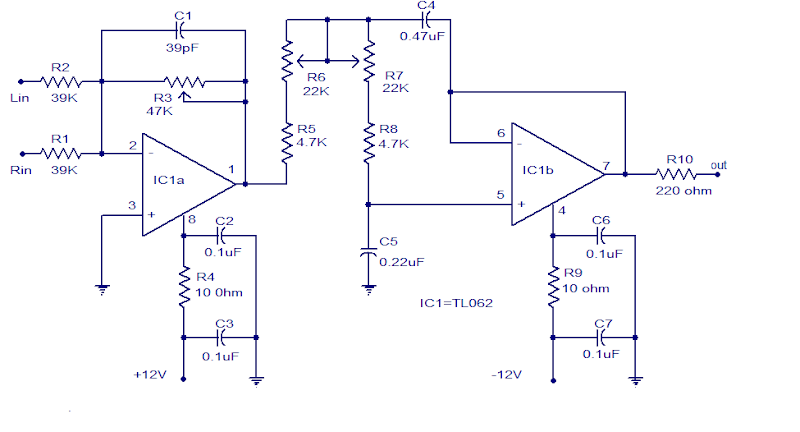
Many low pass filter circuits for subwoofer seem to be given And this is also just Another one. The circuit given here is Depending about the opamp TL062 from one ST Micro electronics. TL062 is really a dual high input impedance J-FET opamp And this has quite low power consumption and high slew rate. The opamp has great audio characteristics and its quite suitable for this circuit.
Out of those two opamps inside TLC062, initial one is wired as the mixer cum pre amplifier stage. The left and right channel seem to be connected in towards the inverting input of IC1a for mixing. The gain of initial stage seem to be either adjusted using POT R3. The output of those initial stage is connected in towards the input of second stage throughout the filter network comprising of components R5,R6,R7,R8,C4 and C5. The second opamp (IC1b) serves as a buffer and the filtered output is at the pin 7 of those TLC062.
Out of those two opamps inside TLC062, initial one is wired as the mixer cum pre amplifier stage. The left and right channel seem to be connected in towards the inverting input of IC1a for mixing. The gain of initial stage seem to be either adjusted using POT R3. The output of those initial stage is connected in towards the input of second stage throughout the filter network comprising of components R5,R6,R7,R8,C4 and C5. The second opamp (IC1b) serves as a buffer and the filtered output is at the pin 7 of those TLC062.
Subscribe to:
Posts (Atom)
