Showing posts with label with. Show all posts
Showing posts with label with. Show all posts
Thursday, November 20, 2014
High HiFi Power Amplifier with MOSFET
Circuit amplifier "High Power HiFi Power Amplifier With MOSFET" is capable of giving the output power to the load speakers 240Watt and 380Watt 8Ohm to load 4Ohm speakers.
Voltage source to a series of power amplifiers "High Power HiFi Power Amplifier With MOSFET" This is a CT 25V 50V 25V to 50V CT of transformer CT. In making this power amplifier needs to be installed heatsinks on the power amplifier (MOSFET) in order to avoid excessive heat. The series of power supply to power amplifer can use the transformer 5A-20A and 35A mounted diode bridge and capacitors for a minimum of 2x 10.000uF electrolit. Details for the power amplifier circuit can be seen in the following figure.
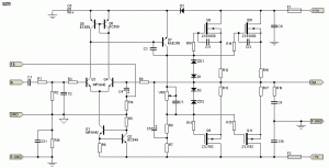
High Power Series HiFi Power Amplifier With MOSFET can modify to increase power output by doubling the final power amplifier is based on the diiginkan. Power generated from doubling the final power amplifier will also double its power output of power amplifier circuit "High Power HiFi Power Amplifier With MOSFET" it.

Fire alarm with light sensor
Fire alarm can be made with a light sensor (LDR) as in the article with the title of Fire Alarm with this LDR sensor. Principles of fire detection Fire Alarm with LDR sensor is to detect the presence of smoke through the LDR. LDR in the series Fire Alarm does not stand alone in detecting a fire, but the LDR in the pair with the light shining on the LDR.
Hence, in the detected smoke from the fire then the intensity of light received by the LDR LDR decreases and eventually trigger an alarm system on a series of Fire Alarm with this LDR sensor. Part 2 that in the series of Fire Alarm with Sensor LDR are some of the sensors, tone generator, audio power.
Image Series Fire Alarm with Sensor LDR

Function Section of the Fire Alarm with Sensor LDR
Part of LDR and light sensor facing to fire smoke detection
Part trigger using transistors and regulators as a trigger tone generator 7805
Tone generator section with IC UM66
Power audio section uses an audio power IC TDA 2002 which is equipped with voleme control (R3)
Wednesday, November 19, 2014
7 Segment Display Digital Dice with IC 4026
7 Segment Display + Digital Dice with IC 4026 -
Composite Materials:
1. IC 555
2. IC 4026
3. 10k ohm resistor (1buah), 100Kohm (1 piece) or replaced with a potentiometer 100k ohms, 220 ohms (7 pieces if necessary)
4. 10 uF capacitor (1 piece)
5. Button press / push button
6. 4.5V battery
7. Jumper cables sufficiently
| 7 Segment Display + Digital Dice with IC 4026 Image |
Assemble steps to Breadboard:
- After stringing understand 555 experimental trials this time it will be easy just follow the schematic drawing shown earlier, and results in the breadboard like this:
- Pushbutton has 4 feet where there are 2 pieces that connect pairs of legs.
- If the battery voltage exceeds 6V, then 7 before going to the 220 ohm resistor required segment or more. If using 4.5 V resistor can not be used.
- Play-turn potentiometer to obtain the desired rate of addition of digits.
- If speed digit changes very quickly, then the circuit can be used as "ELECTRONIC DICE". So when the button is pressed it will stop the numbers digit number we do not expect before.
There is info of 7 Segment Display + Digital Dice with IC 4026
Tuesday, November 18, 2014
Multiplexer with CMOS IC 4556
In addition to the family of TTL ICs that support the function of a multiplexer is a family of CMOS ICs.

Read More..
Despite the fact it is the family of TTL ICs that support more functions than the CMOS multiplexer. For the working principle of the multiplexer IC CMOS family is actually tantamount to a multiplexer circuit, or IC TTL logic gates. That should be all referring to the real multiplexer function, namely the determination of output lines which represent the number of input lines. The use of symbols is possible between TTL and CMOS IC has a different but actually run the same rules. For your reference if you are interested in using family of CMOS IC 4556 series in particular, I include also the truth table below:
INPUT | OUTPUT | |||||
E | A0 | A1 | O0 | O1 | O2 | O3 |
L | L | L | L | H | H | H |
L | H | L | H | L | H | H |
L | L | H | H | H | L | H |
L | H | H | H | H | H | L |
H | X | X | H | H | H | H |
L = LOW | ||||||
H = HIGH | ||||||
Tuesday, November 11, 2014
LED flasher with Transistor circuits Diagram
These circuits only flash one or two LEDs. This is opposed to the light chaser circuits that can flash four or more. Of course, the simplest LED flasher is simply to use a flashing LED. The problem with that approach is you have no control over the flash rate, but it does have its use for eye catching displays for selling stuff. The circuits below give you that control, plus they can flash two LEDs alternately.
There are many possible applications for the circuits below, especially for kids, who love flashing lights. Heres some possible uses.
- Railroad crossing signal for model railroads.
- Safety blinkers for bicycles, etc.
- Fun stuff for Halloween, like making those plastic Jack-O-lanterns blink (try using ultraviolet LEDs here).
- Christmas decorations.
- Blinkers to locate items in the dark.
Transistor LED flasher
This circuit has a lot going for it. For one thing, it only consists of two transistors, two capacitors and four resistors. That also means it consumes very little power. You can control the flash rate by changing the size of the 100k resistors (100k makes for a pretty slow rate). You can also control the duty cycle by using resistors of different values on the two sides. The 470 ohm resistors control the current through the LEDs. Normally you want to limit this to 20mA, but to conserve battery power, you may need to limit it even further. You can also connect several LEDs in series, instead of using only one for each side. With red LEDs (1 per side) and the values shown, the circuit draws about 11mA. Heres what the actual circuit looks like:
On this circuit, the green wires connect to the LEDs, but you can mount them on the actual circuit board for some applications. The picture is about twice actual size.
Sunday, November 2, 2014
2×25W Stereo Power Amplifier with STK4141II
2×25W Stereo Power Amplifier with STK4141II

Recommended voltage is 27.5V for 8ohms speaker and 24.5V for 4ohms speaker while the maximum voltage to supply this circuit should be about 41 VDC.
Heatsink usage on the power IC is a must.
Use this STK4141II Datasheet for your reference.
LMC7101 LMC7101Q TINY AMPLIFIER WITH RAIL TO RAIL INPUT OUTPUT ELECTRONIC DIAGRAM

LMC7101 - LMC7101Q TINY AMPLIFIER WITH RAIL-TO-RAIL INPUT-OUTPUT ELECTRONIC DIAGRAM
The performance is similar to a single amplifier of the LMC6482/LMC6484 type, with rail-to-rail input and output, high open loop gain, low distortion, and low supply currents. The main benefits of the Tiny package are most apparent in small portable electronic devices, such as mobile phones, pagers, notebook computers, personal digital assistants, and PCMCIA cards.
Sunday, October 26, 2014
LED Lights circuits with LM339 IC555
This circuit reproduces the opening light sequence now used by FISA instead of Formula individual racing. It may possibly befall used with slot car sets (such like HO shin up AFX/Life Like/Tyco sets) or else means of communication controlled cars. IC1, a 555 timer IC, is used as a meter pulse generator. Its output is fed via NAND gates IC2a and IC2c to IC3, a 4024 binary counter. IC2b inverts the O4 output of 4024 binary counter IC3. at first, IC3 is reset and all its outputs are low, together with O4, which causes IC2b to grant a commonsensical climax to the pin 8 input of IC2c which afterward passes pulses from the 555 timepiece circuit to the clock input of the 4024. IC3 then begins including.
Similar to the count has reached binary 1111, the then pulse sends the O4 output of IC3 high, which disables IC2c and IC3 stops together with. The four used outputs of IC3 are connected to a resistor ‘ladder’ which acts because a undemanding digital to analog convert-er (DAC). As the count increases so does the voltage produced by the top of the ladder and this is connected to the inverting inputs of four comparators inside IC4 (an LM339) and to IC5, which is a 741 op amp besides connected for instance a comparator.
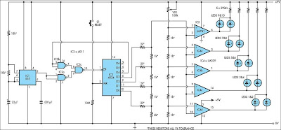
The certain inputs of the comparators are connected to the taps of a voltage barrier, with the drumming voltages frozen using VR1, a 100kO trimpot. As IC3 counts, the rising stepped voltage from the DAC ladder switches the comparators on during sequence, preparatory with IC4d and working up to IC5. because each one comparator is bowed on, its put together of LEDs is lit; essential LEDs 1 & 2, so therefore LEDs 3 & 4 and so on. at what time all five pairs of LEDs are lit, the after that pulse from IC1 moves the binary count of IC3 to 10000, so the DAC voltage drops back to zip and all LEDs are extinguished. by the same age, plus additionally stops, as the lofty on O4 causes IC2c to mass expand gate pulses. The circuit it follows that remains stationary until the counter is reset by burning pushbutton switch S1. This allows a new-fangled sequence to kick off.
Similar to the count has reached binary 1111, the then pulse sends the O4 output of IC3 high, which disables IC2c and IC3 stops together with. The four used outputs of IC3 are connected to a resistor ‘ladder’ which acts because a undemanding digital to analog convert-er (DAC). As the count increases so does the voltage produced by the top of the ladder and this is connected to the inverting inputs of four comparators inside IC4 (an LM339) and to IC5, which is a 741 op amp besides connected for instance a comparator.

The certain inputs of the comparators are connected to the taps of a voltage barrier, with the drumming voltages frozen using VR1, a 100kO trimpot. As IC3 counts, the rising stepped voltage from the DAC ladder switches the comparators on during sequence, preparatory with IC4d and working up to IC5. because each one comparator is bowed on, its put together of LEDs is lit; essential LEDs 1 & 2, so therefore LEDs 3 & 4 and so on. at what time all five pairs of LEDs are lit, the after that pulse from IC1 moves the binary count of IC3 to 10000, so the DAC voltage drops back to zip and all LEDs are extinguished. by the same age, plus additionally stops, as the lofty on O4 causes IC2c to mass expand gate pulses. The circuit it follows that remains stationary until the counter is reset by burning pushbutton switch S1. This allows a new-fangled sequence to kick off.
Friday, October 24, 2014
Toggle Switch with IR
Toggle switch in this article is a series of toggle switches that are controlled by infrared light. The series toggle switch is made from a combination of data flip-flop CD4013 2 units. Receiver circuit of the infrared light signals arranged with infrared receiver as found on television remote receiver. Infrared signal from remote is used as clock signals and data to the data flip-flop first. then the second flip-flop data set as a toggle flip-flop toggle the output signal is used to drive the relay. for more details can be seen in thethe following image .

Series Toggle Switch With Infra Red (IR) that is required to supply voltage range of 12VDC and the output of Toggle Switch With Infra Red (IR) is dapt used to turn on the lights or other electronic devices with DC or AC voltage source. Series Toggle Switch With Infra Red (IR) was isolated from the load that is placed for use as the final relay.
Subwoofer Amplifier with STK4241V
The Subwoofer Amplifier based STK4241V was posted by in the sphere of kind Amplifier. Please examine suspiciously and look by the side of schematic design photos of Subwoofer Amplifier based STK4241V to achieve note in a row.

Read More..

This Subwoofer Amplifier is equiped with STK4241V wich is a clot avenue intercrossed IC, AF Cognition Amplifier (Separate Superpower action) (120W+120W min, THD = 0.08%). STK4241V has not many skin tone analogous: Muting circuit built-participating in to padding all types of puzzlement disturbance, spanking mirror track on behalf of low 0.08% corps sweet form. For this 2×120W state stereo alphabetical listing oftenness amplifier we draw on a sole monochip STK4241V to attain up to 120W for both transmission.
Sunday, October 19, 2014
Multiplexer Circuit With Logic Gate
Multiplexer circuit with a logic gate is a multiplexer circuit that utilizes a combination of logic gates.

The working principle of the multiplexer circuit above is:
1. Value of bit 00 from the selector will choose the path of the first input as the output
2. Value of bit 01 of the selector will choose the path of the second input as output
3. Value of bit 10 of the selector selects the third input lines as output
4. Value of bit 11 of the selector will choose the four input channels as output
5. As long as there is no change in the bit selector logic condition of the output logic state also will not be amended.
6. If the line selector is connected with a series of counter-up the output to be obtained will represent the input lines in sequence.
7. So it can be concluded that the usefulness of the implementation of a multiplexer function is to satisfy the principle of a simple data distribution. Thus, with multiplexers is possible to transmit data remotely using only one connection.
Read More..
Where the above example can be seen that the circuit has 2 bit selector and 4 input lines. You can make a circuit with more input channels by increasing the number of bits of the selector. And also you can use a combination of gates based on your own design with reference to the previous multiplexer truth table you should specify. So by making a truth table in advance you can easily create a series of logic gates.
The working principle of the multiplexer circuit above is:
1. Value of bit 00 from the selector will choose the path of the first input as the output
2. Value of bit 01 of the selector will choose the path of the second input as output
3. Value of bit 10 of the selector selects the third input lines as output
4. Value of bit 11 of the selector will choose the four input channels as output
5. As long as there is no change in the bit selector logic condition of the output logic state also will not be amended.
6. If the line selector is connected with a series of counter-up the output to be obtained will represent the input lines in sequence.
7. So it can be concluded that the usefulness of the implementation of a multiplexer function is to satisfy the principle of a simple data distribution. Thus, with multiplexers is possible to transmit data remotely using only one connection.
Wednesday, October 15, 2014
Build a High And Low Voltage Cut Off With Time Delay Circuit Diagrams
The power line fluctuations and cut-offs cause damages to electrical appliances connected to the line. It is more serious in the case of domestic appliances like fridge and air conditioners. If a fridge is operated on low voltage, excessive current flows through the motor, which heats up, and get damaged.
The under/over voltage protection circuit with time delay presented here is a low cost and reliable circuit for protecting such equipments from damages. Whenever the power line is switched on it gets connected to the appliance only after a delay of a fixed time. If there is hi/low fluctuations beyond sets limits the appliance get disconnected. The system tries to connect the power back after the specific time delay, the delay being counted from the time of disconnection. If the power down time (time for which the voltage is beyond limits) is less than the delay time, the power resumes after the delay: If it is equal or more, then the power resumes directly.
This circuit has been designed, built and evaluated by me to use as a protector for my home refrigerator. This is designed around readily available semi-conductor devices such as standard bipolar medium power NPN transistor (D313/SL100/C1061), an 8-pin type 741 op-amp and NE555 timer IC. Its salient feature is that no relay hunting is employed. This draw back is commonly found in the proctors available in the market.
The complete circuit is consisting of various stages. They are: - Dual rail power supply, Reference voltage source, Voltage comparators for hi/low cut offs, Time delay stage and Relay driver stage. Lets now look at the step-by-step design details.
Dual rail power supply.
This is a conventional type of power supply as shown in Figure 1. The power is applied through the step-down transformer (230/12-0-12V/500mA). The DC proportional to the charging input voltage is obtained from bridge rectifier. Two electrolytics are there to bypass any spikes present. Bridge is capable of handling currents up to 1 Amp.
Output is given by: -
V(out) = 0.71 X V (secondary)
= 0.71 X 24V
= 17.04 V
(This equation is similar for the negative rail as well)
This is a conventional type of power supply as shown in Figure 1. The power is applied through the step-down transformer (230/12-0-12V/500mA). The DC proportional to the charging input voltage is obtained from bridge rectifier. Two electrolytics are there to bypass any spikes present. Bridge is capable of handling currents up to 1 Amp.
Output is given by: -
V(out) = 0.71 X V (secondary)
= 0.71 X 24V
= 17.04 V
(This equation is similar for the negative rail as well)
Circuit diagram

Low voltage cut off op-amp
Figure 2 shows the use of very common and easily available op-amp 741 as a comparator. The op-amp is available in TO-5 and DIP type packing.
Figure 2 shows the use of very common and easily available op-amp 741 as a comparator. The op-amp is available in TO-5 and DIP type packing.
Circuit diagram

In this ckt the zener diode D1 and it’s associated resistor R1 are connected to the non-inverting terminal (+ve) of 741 to give the suitable reference voltage. The DC voltage from the sensor is given to the inverting (-ve) terminal through pre-set R2.This is used to set the input level.
When the sensor input is less than Zener voltage the output from the Op-amp remains high and when it is greater than Zener voltage the output goes low. When the sensing voltage is equal to Zener voltage the output of the op-amp is approximately zero.
This phenomenon is used as a decision for switching the relay and to give cutoff in a low voltage situation.
When the sensor input is less than Zener voltage the output from the Op-amp remains high and when it is greater than Zener voltage the output goes low. When the sensing voltage is equal to Zener voltage the output of the op-amp is approximately zero.
This phenomenon is used as a decision for switching the relay and to give cutoff in a low voltage situation.
High voltage cut off op-amp
Here the op-amp is used as a inverted amplifier. See Figure 3.Zener and resistor network gives reference voltage to the inverting terminal (-ve) of op-amp. Sensing voltage derived through the 10 K pre-set is given to the non- inverting (+ve) terminal and this sets the high level cut.
Here the op-amp is used as a inverted amplifier. See Figure 3.Zener and resistor network gives reference voltage to the inverting terminal (-ve) of op-amp. Sensing voltage derived through the 10 K pre-set is given to the non- inverting (+ve) terminal and this sets the high level cut.
When the input DC from the sensor is less than Zener voltage the output of the op-amp is low and vice-versa. When the input DC voltage is equal to the zener voltage, the op-amps output is approximately zero.
Circuit diagram

Time delay
I’ve selected the 555 timer due to following reasons.
1. Timing from microseconds through hours.
2. Ability to operate from wide range of supply voltages.
3. High temperature stability.
4. Easily Available.
5. Its triggering circuit is quite sensitive.
I’ve selected the 555 timer due to following reasons.
1. Timing from microseconds through hours.
2. Ability to operate from wide range of supply voltages.
3. High temperature stability.
4. Easily Available.
5. Its triggering circuit is quite sensitive.
This is basically a monostable. The external timing capacitor C2 is held initially discharged by the timer. The circuit triggers upon receiving a pulse to its pin 2 when the level reaches 1/3 Vcc. Once triggered., the circuit will remain in that state until the set time is elapsed or power to the circuit cuts off. The delayed period in seconds is 1.1 C2.R1 where R1 is in megohms and C2 is in microfarads. In practice, R1 should not exceed 20 M. If you use an electrolytic capacitor for C2, select a unit for low leakage. The time delay may have to be adjusted by varying R1 to compensate for the wide tolerance of electrolytics.
Circuit diagram

Relay Driver
The output from the voltage level detectors cannot directly drive the relay and hence the relay driver is used.
The output from the voltage level detectors cannot directly drive the relay and hence the relay driver is used.
Circuit diagram

In this a relay (12V <500 ohms) is connected to the collector of npn transistor. the out put voltage from the comparator is applied to the base of npn transistor through a resistance r1. when the output from the comparator is low the transistor is in off state and the relay is in de-energized state. similarly when the output from the comparator goes high the transistor switches on and the flow of current from the collector to emitter of transistor energizes the relay.
Generally in a relay driver circuit, parallel to the relay coil, a diode or a capacitor is used. This is to eliminate the back e.m.f generated by the relay coil when currents are suddenly broken. Capacitor C1 is connected in parallel to the coil, which filters out the back emf but it, slows down the working of relay.
A better method is to connect two diodes (as shown in the figure 5) that stop the relay – transistor junction swinging more than 600mV above the positive rail or below the zero-volt rail. During normal operation the diodes are reverse biased and have no effect on the performance of circuit. But when back emf is induced, the diodes conduct heavily and absorb all transient voltages. However, I have employed the both methods.
The Complete Circuit
Circuit diagram

Under normal operating conditions i.e. when the input voltage is between maximum and minimum limit the output from the both the comparators are low. The transistor Q1 is OFF and the relay is in de-energized (pole connected to N/C pin) state and the output is obtained.
When the input voltage is below or above the limits set by the pre-sets R8 or R9, the output of the Op-Amps goes either low or high and diodes D1 or D2 would be forward biased depending on the situation. Transistor Q1 switches ON and the flow of current from collector to emitter energizes the relay and the output is cutoff.
A small amount of hystersis has been added via feed back resistors R10 & R11 so that the relay turns on when the level falls to a particular value but does not turn again until it raises a substantial amount above this value. Other wise the relay contacts will frequently turn on/off and produce chattering.
Construction Hints
1) I used a piece of varoboard, which has copper strips on one side to mount the components, and housed the entire circuit and the transformer in a discarded ATX PC power supply box.
1) I used a piece of varoboard, which has copper strips on one side to mount the components, and housed the entire circuit and the transformer in a discarded ATX PC power supply box.
2) An autotransformer has been used to set the limits. Set the output of the autotransformer to 250V AC and connect it to the primary of transformer T1 (see Figure 1). Then adjust the pre-set R9 such that relay just energizes. This is the high limit. Next set the output of the autotransformer to 200V AC and adjust the pre-set R8 such that the relay energizes. Please note that these are my preferred limits but you may select any range from say 170 to 270V AC.
3) A neon with a suitable resistor could be connected between the AC supply lines as an ON indicator. Alternatively, LED with a current limiting resistor could be connected between the relay coil so when the relay is energized LED will indicate the situation.
Tuesday, October 14, 2014
MOSFET IRF540 based 100W 12VDC to 220VAC Inverter diagram
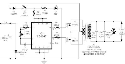
The following inverter circuit is using MOSFET transistor IRF540 instead of ordinary transistor (eq 2N3055). FET is better than ordinary transistor in both stability and responsibility.
Sunday, September 21, 2014
Amplifier simple easy and cheap with IC TA7368P
Indeed , this amplifier is suitable known as the title above. Viewed from the schematic alreaady seen that this amplifier circuit requires little components and parts were cheap. This amplifier requires 1 piece of IC TA7368P is manufactered by TOSHIBA is the price too low, then in addition to IC amplifier requires 3 components elco capacitor whose value is not too big. Maybe if you make this amplifier circuit, the total price of all must not be more than $ 1. This amplifier only has more than 1W output, perhaps because it has little strengthening it so that the output is released is very small. But to make this is quite easy and not too costly.
Capacitor
C1 = 100 uF
C2 = 100uF
C3 = 470uF
IC
IC1 = TA7368P
Good Luck :)
Thursday, September 18, 2014
Car audio amplifier with IC TA7203P
Circuit Diagram
 |
| Car audio amplifier with IC TA7203P |
Circuit Description
Stereo car power amplfier with TA7203P , is suitable for the room your car , your car it will build an increasingly crowded and felt like using high-class amplifiers and speakers. Simply using this circuit and some speaker subwoofer speakers you can enjoy it.
Technical information :
- Max voltage = 20 Volt
- Min voltage = 8 Volt
- Max output = 2 x 40 Watt
- RL = 8 Ohm
Tuesday, September 16, 2014
60W ICs amplifier with OM961
Amplifier circuit is very suitable for use in car audio speakers that use a subwoofer, with a power output of about 60W and impedance of 4 Ohm. Supply voltage ranging from 12V to 35 volts with currents +, -, and ground. If using battery then use 12V DC to DC converter which produces 3 voltage +, -, and ground.
Guitar Circuit with built in speaker
The idea to make a guitar with a built-in speaker came when I stumbled upon a fact that if I miss a pulse through the speaker, it will be heard far away.
Recall manual siren. Human hand, twisting it develops 0.1 horsepower, this is where it is 100 watts (RMS), and heard it on the entire city.Flashlight compared with 1500 Watt PMPO 1000W RMS projector brightness turned this flashlight shines brighter and more, even though there was a light bulb 5 watts RMS. Similarly, energy saving light bulbs, written on them two 100 watts and 8 watts. But this retreat. Also on imported musical instrument in writing all power PMPO.
So, if the distortion of the sound spectrum converted to a pulse with a large buildup of small capacitors and alleviate sinus large capacitors, then turn out so when mixed. Promoduliruyutsya under sinusoidal pulses, acquiring the height of its envelope. Pulses will hear anything away, because of their large growth. But due to the fact that they will have different heights under sinus, they will be perceived by the human ear differently, carrying information about the full spectrum of sound.
This transformation into pulses and sine and mixing occurs on a chip amplifier effective D2 (the chip I can not seem to pick up for this part, so did its own microassembly until painted, because it developed). Coefficient PMPO this chip gives the coefficient 300. That is, when consumption of battery power amplifier crown 0.8 watts (RMS) guitar gives out 240 Watts PMPO volume.
Scheme guitar with built-in speaker:

It is known that it is necessary for restaurants 100 watts to 300 watts shift halls (power amplifier goes 1 Watt RMS) for concert 1000 watt (power amplifier here goes 3.3 watts RMS). Coefficient PMPO 300 guitar can do it.
This part of the effective amplifier with limiting diodes D2 purely mine. The first part of the effective amplifier, tone and preamp made by conventional schemes. Power Amplifier taken from Marshall amp already built up a guitar at a frequency of 50 to 13,500 Hz. Did not want to reinvent the wheel.
The third chip preamplifier (preamp), stands for alignment voltage DC tone, if it comes to it a little, as well as for the formation of overdrive. If humps AFC voices raised high, they begin to be limited, there is an increase in their growth, rather than amplitude. Intermediate frequencies are soft, not isolated and then there is no loss spectrum and volume control on the ear remains.
D2 tuned to the frequency 1700 - 2200 Hz and generates downs 100 to 3500-4500 Hz. Input from 2 to 5 millivolts it does not distort.
Frequency obstructions on different chains, plus a capacitor input impedance or resistance, etc. I want to calculate, but a book with formulas passed back to the Institute, it is necessary to take it again. While doing the ear, with observations from other circuits and devices.Infringement at low frequencies not, because it is necessary for the effects of sound from 100 Hz, body volume allows guitars to make them.
The sound of this scheme, because such characteristics can be confused with the sound of bands such as Disi Asay, Metallica, Gaunz Roses, Kiss, Bon Jovi. It all depends on the setting of D2, and can be customized to fit our music. It adjusts for distoshn, drive, metal, electrical, acoustic, mixed. Channels are made entirely only without amplifier and the first part of the amplifier efficiently. In the diagram this channel is highlighted with a blue border.
That makes guitars with a slightly shorter scale length with pegs on the other side, that would have been smaller sizes. I think the small size would blend well with a large capacity.
Sunday, September 14, 2014
Power amplifier compatible with TV audio

In this amplifier circuit using IC TDA8944J as the main amplifier with dual-channel audio amplifier with 2 x 7W output power at 8 Ω impedance. And a minimum supply voltage of 9-18 Volts. In this ic contains two Bridge Tied Load or BTL amplifier.
The circuit is often found in audio amplifier in a series of television, besides TDA2003, TDA2006 and so forth. PCB for a series of amplifiers using IC TDA8944J is very compatible with all other types of IC in IC TDA894X family unit , and below is a schematics.
Saturday, September 13, 2014
16 × 2 LCD Volt Meter Ampere Meter With PIC
Volt meters & ampere meter with PIC can be used to measure voltage and current simultaneously. The series of volt meters & ampere meter with PIC16F876A PIC is used as a data processor voltage and current are measured.
This circuit uses the viewer in the form of 16 × 2 LCD used for the data display voltage and current measurements. In the article volt meter and ampere meter with PIC are discussed kerannya limited to devices only. More detail can be seen from the image sequence volt meter and ampere meter with PIC below.
The images of Volt Meter & Ampere Meter With PIC Circuit
 |
| Volt meters & ampere meter with PIC |
Tuesday, September 2, 2014
Digital Thermometer with data processing of a microcontroller AT89C4051
Digital Thermometer 0-100.0°C is a digital thermometer that operates in modetemperature measurement in Celsius (° C). Digital Thermometer 0-100.0 ° C in this article uses data processor in the form of a microcontroller AT89C4051.
Temperature sensors used in Digital Thermometer 0-100.0 ° C. This temperature sensor LM35D. Digital Thermometer 0-100.0 ° C. It uses the temperature measurement data viewer in the form of 1 line LCD viewer. Digital Thermometer 0-100.0 ° C. It can display the temperature measurement data with a resolution of 0.1 ° C.
Temperature sensors used in Digital Thermometer 0-100.0 ° C. This temperature sensor LM35D. Digital Thermometer 0-100.0 ° C. It uses the temperature measurement data viewer in the form of 1 line LCD viewer. Digital Thermometer 0-100.0 ° C. It can display the temperature measurement data with a resolution of 0.1 ° C.
| Digital Thermometer Circuit Diagram |
Digital Thermometer 0-100.0 ° C. These temperature sensors make use of LM35D as temperature sensing. In Digital Thermometer 0-100.0 ° C. This temperature sensor measurement data this LM35D (Level Voltage) is then converted into 4-bit binary data using the ADC CA3162.
Then the 4-bit data from ADC CA3162 which is a measurement of data if the temperature is in the AT89C4951 microcontroller so that it becomes an operating principle of temperature measurement based on digital thermometers. In the final stage of the Digital Thermometer 0-100.0 ° C. This is the appearance of digital data temperature measurement, using digital data viewer of the LCD 1 line.
Then the 4-bit data from ADC CA3162 which is a measurement of data if the temperature is in the AT89C4951 microcontroller so that it becomes an operating principle of temperature measurement based on digital thermometers. In the final stage of the Digital Thermometer 0-100.0 ° C. This is the appearance of digital data temperature measurement, using digital data viewer of the LCD 1 line.
Subscribe to:
Posts (Atom)
