Showing posts with label 3. Show all posts
Showing posts with label 3. Show all posts
Wednesday, November 5, 2014
High Voltage 3 Watt Audio Power Amplifier
The LM4954 is an audio power amplifier primarily designed for demanding applications in mobile phones and other portable communication device applications. It is capable of delivering 2.4 Watts of continuous average power to an 8 BTL load with less than 1% THD+N from a 7VDC power supply. Boomer audio power amplifiers are designed specifically to provide high quality output power with a minimal number of external components. The LM4954 does not require output coupling capacitors or bootstrap capacitors, and therefore is ideally suited for lower-power portable applications where minimal space and power consumption are primary requirements.
BTL load with less than 1% THD+N from a 7VDC power supply. Boomer audio power amplifiers are designed specifically to provide high quality output power with a minimal number of external components. The LM4954 does not require output coupling capacitors or bootstrap capacitors, and therefore is ideally suited for lower-power portable applications where minimal space and power consumption are primary requirements.High Voltage 3 Watt Audio Power Amplifier Circuit Diagram
The LM4954 features a low-power consumption global shutdown mode which is achieved by driving the shutdown pin with logic low. Additionally, the LM4954 features an internal thermal shutdown protection mechanism.
The LM4954 contains advanced pop & click circuitry which eliminates noises that would otherwise occur during turn-on and turn-off transitions.
The LM4954 is unity-gain stable and can be configured by external gain-setting resistors.
Key Specification:
| Wide Power Supply Voltage Range | 2.7 <= VDD <= 9V |
| Output Power: VDD = 7V, 1% THD+N | 2.4W (typ) |
| Quiescent power supply current | 3mA (typ) |
| PSRR: VDD = 5V and 3V at 217Hz | 80dB (typ) |
| Shutdown power supply current | 0.01µA (typ) |
Features:

Monday, November 3, 2014
Universal Tester for 3 pin Devices
Most 3-terminal active components can be tested statically using just an ohmmeter. But when you have a lot of these devices to test, the procedure soon becomes boring. That’s where the idea came from to combine fast, easy testing for these types of device into a single instrument.
The unit described here enables you to test NPN and PNP bipolar transistors, N-or Pchannel FETs or MOSFETs, UJTs, triacs, and thyristors. Regardless of the type of device, the tests are non-destructive. Universal connectors allow testing of all package types, including SMDs (up to a point). The unit lets you change from one type of device to another in a trice. It avoids using a multi-pole switch, as they’re too expensive and hard to find.
Universal Tester for 3-pin Devices Circuit diagram:
Here’s how to build a versatile instrument at a ridiculously low cost. IC1 is a 4066 quad CMOS switch which will let us switch between bipolar transistors and FETs. LEDs D1–D4 tell us about the condition of the test device, when we press the ‘Test’ button. The 4066 can only handle a few milliamps, not enough for the other component types to be tested, hence the reason for using relay RE1. This 12 V relay offers two NO contacts. The first applies power to the UJT test circuit, the second applies it to the triac and thyristor test circuit.
Extensive testing has shown that the best way to test UJT transistors is to do so dynamically, with the help of a relaxation oscillator. Net-work R11/C1 sets the oscillator frequency to around 2 Hz. On pin B1 of the UJT we find a nice sawtooth, which is not of much interest to us here. However, pin B2 gives good but very short pulses. IC2, wired as a monostable, lengthens these pulses so they can be clearly seen via LED D5.
The relay’s second pole is going to drive the thyristor’ sortriac’s trigger pin. The value of R18 is a good compromise with respect to the varying trigger currents for this type of device. Resistor R17 is important, as the hold-ing current must be high enough for a triac; 250 mA is a good compromise. LED D6 tells you if the device is in good condition or not; but watch out, the test result must be con-firmed by briefly cutting the power in order to reset the triac.
On the web page for this article [1] you’ll find the author’s CAD files (PCB layout and front panel) along with some photos of his project. On the prototype, the LEDs and the ‘Test’ button were wired onto the copper side of the PCB. The six female connectors for the devices being tested were salvaged, but there are lots of models available on the market (the pitch is standard). The test cable crocodile clips must be as small as possible for testing SMD devices.
Friday, September 12, 2014
Simple 3 Input and Gate Comparator Wiring diagram Schematic
This is a Simple 3 Input and Gate Comparator Circuit Diagram. This schema has high output only when all three inputs are high. The non inverting-input current, when all three inputs are high, must exceed that of the inverting input, as determined by R4. The schema can be converted to a AND gate by transposing the two inputs of the op amp.
3 Input and Gate Comparator Circuit Diagram
![3]()
3 Input and Gate Comparator Circuit Diagram
Friday, August 15, 2014
Build a 3 Watt Stereo Amplifier Wiring diagram Schematic
Build a 3 Watt Stereo Amplifier Circuit Diagram. This schema using MAX 7910 IC. The MAX9710 a stereo audio power amplifier IC capable of delivering 3Watts of out put to 4 Ohm loads. MAX9710 can be operated from a single 4.5V to 5.5V power supply , makes it ideal for hand held applications.The IC for
3 Watt stereo amplifier schema also features thermal overload protection.
3 Watt Stereo Amplifier Circuit Diagram
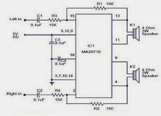
This 3 Watt stereo amplifier schema is suitable for small power audio devices such as radio sets and portable CD players. 5 V DC power supply is used for powering the 3 Watt stereo amplifier schema. 6V battery with an IN 4007 diode series to the positive terminal of it can also be used instead of 5 V DC supply. The 3 Watt stereo amplifier schema will get a supply voltage approximately 5 V after 0.7 V voltage drop across diode.
Subscribe to:
Posts (Atom)
