Showing posts with label high. Show all posts
Showing posts with label high. Show all posts
Thursday, November 20, 2014
High HiFi Power Amplifier with MOSFET
Circuit amplifier "High Power HiFi Power Amplifier With MOSFET" is capable of giving the output power to the load speakers 240Watt and 380Watt 8Ohm to load 4Ohm speakers.
Voltage source to a series of power amplifiers "High Power HiFi Power Amplifier With MOSFET" This is a CT 25V 50V 25V to 50V CT of transformer CT. In making this power amplifier needs to be installed heatsinks on the power amplifier (MOSFET) in order to avoid excessive heat. The series of power supply to power amplifer can use the transformer 5A-20A and 35A mounted diode bridge and capacitors for a minimum of 2x 10.000uF electrolit. Details for the power amplifier circuit can be seen in the following figure.
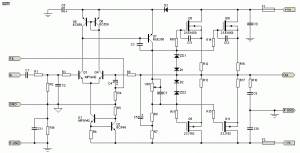
High Power Series HiFi Power Amplifier With MOSFET can modify to increase power output by doubling the final power amplifier is based on the diiginkan. Power generated from doubling the final power amplifier will also double its power output of power amplifier circuit "High Power HiFi Power Amplifier With MOSFET" it.

Tuesday, November 18, 2014
10A High Current variable power supply
Power supply has 10A maximum current and output voltage can be set from 2 - 36VDC. Power supply circuit is quite simple, which is composed of the rectifier, voltage regulator and power regulator. Power regulator circuit High Current Variable Power Supply 10A uses the Q3 and Q4 are arranged Darlington and serves as a power regulator drivers Q5 and Q6. While the voltage regulator circuit is VR1 which serves as a variable voltage divider and Q1 and Q2 are arranged as a controller driver Darlington power regulator with variable reference voltage divider VR1.
In a series of High Current Variable Power Supply 10A 10A above have been completed as a current-limiting fuse. and to monitor the current flowing with ampere meter and volt meter to monitor the output voltage of the circuit.
Wednesday, November 5, 2014
High Voltage 3 Watt Audio Power Amplifier
The LM4954 is an audio power amplifier primarily designed for demanding applications in mobile phones and other portable communication device applications. It is capable of delivering 2.4 Watts of continuous average power to an 8 BTL load with less than 1% THD+N from a 7VDC power supply. Boomer audio power amplifiers are designed specifically to provide high quality output power with a minimal number of external components. The LM4954 does not require output coupling capacitors or bootstrap capacitors, and therefore is ideally suited for lower-power portable applications where minimal space and power consumption are primary requirements.
BTL load with less than 1% THD+N from a 7VDC power supply. Boomer audio power amplifiers are designed specifically to provide high quality output power with a minimal number of external components. The LM4954 does not require output coupling capacitors or bootstrap capacitors, and therefore is ideally suited for lower-power portable applications where minimal space and power consumption are primary requirements.High Voltage 3 Watt Audio Power Amplifier Circuit Diagram
The LM4954 features a low-power consumption global shutdown mode which is achieved by driving the shutdown pin with logic low. Additionally, the LM4954 features an internal thermal shutdown protection mechanism.
The LM4954 contains advanced pop & click circuitry which eliminates noises that would otherwise occur during turn-on and turn-off transitions.
The LM4954 is unity-gain stable and can be configured by external gain-setting resistors.
Key Specification:
| Wide Power Supply Voltage Range | 2.7 <= VDD <= 9V |
| Output Power: VDD = 7V, 1% THD+N | 2.4W (typ) |
| Quiescent power supply current | 3mA (typ) |
| PSRR: VDD = 5V and 3V at 217Hz | 80dB (typ) |
| Shutdown power supply current | 0.01µA (typ) |
Features:
Wednesday, October 15, 2014
Build a High And Low Voltage Cut Off With Time Delay Circuit Diagrams
The power line fluctuations and cut-offs cause damages to electrical appliances connected to the line. It is more serious in the case of domestic appliances like fridge and air conditioners. If a fridge is operated on low voltage, excessive current flows through the motor, which heats up, and get damaged.
The under/over voltage protection circuit with time delay presented here is a low cost and reliable circuit for protecting such equipments from damages. Whenever the power line is switched on it gets connected to the appliance only after a delay of a fixed time. If there is hi/low fluctuations beyond sets limits the appliance get disconnected. The system tries to connect the power back after the specific time delay, the delay being counted from the time of disconnection. If the power down time (time for which the voltage is beyond limits) is less than the delay time, the power resumes after the delay: If it is equal or more, then the power resumes directly.
This circuit has been designed, built and evaluated by me to use as a protector for my home refrigerator. This is designed around readily available semi-conductor devices such as standard bipolar medium power NPN transistor (D313/SL100/C1061), an 8-pin type 741 op-amp and NE555 timer IC. Its salient feature is that no relay hunting is employed. This draw back is commonly found in the proctors available in the market.
The complete circuit is consisting of various stages. They are: - Dual rail power supply, Reference voltage source, Voltage comparators for hi/low cut offs, Time delay stage and Relay driver stage. Lets now look at the step-by-step design details.
Dual rail power supply.
This is a conventional type of power supply as shown in Figure 1. The power is applied through the step-down transformer (230/12-0-12V/500mA). The DC proportional to the charging input voltage is obtained from bridge rectifier. Two electrolytics are there to bypass any spikes present. Bridge is capable of handling currents up to 1 Amp.
Output is given by: -
V(out) = 0.71 X V (secondary)
= 0.71 X 24V
= 17.04 V
(This equation is similar for the negative rail as well)
This is a conventional type of power supply as shown in Figure 1. The power is applied through the step-down transformer (230/12-0-12V/500mA). The DC proportional to the charging input voltage is obtained from bridge rectifier. Two electrolytics are there to bypass any spikes present. Bridge is capable of handling currents up to 1 Amp.
Output is given by: -
V(out) = 0.71 X V (secondary)
= 0.71 X 24V
= 17.04 V
(This equation is similar for the negative rail as well)
Circuit diagram

Low voltage cut off op-amp
Figure 2 shows the use of very common and easily available op-amp 741 as a comparator. The op-amp is available in TO-5 and DIP type packing.
Figure 2 shows the use of very common and easily available op-amp 741 as a comparator. The op-amp is available in TO-5 and DIP type packing.
Circuit diagram

In this ckt the zener diode D1 and it’s associated resistor R1 are connected to the non-inverting terminal (+ve) of 741 to give the suitable reference voltage. The DC voltage from the sensor is given to the inverting (-ve) terminal through pre-set R2.This is used to set the input level.
When the sensor input is less than Zener voltage the output from the Op-amp remains high and when it is greater than Zener voltage the output goes low. When the sensing voltage is equal to Zener voltage the output of the op-amp is approximately zero.
This phenomenon is used as a decision for switching the relay and to give cutoff in a low voltage situation.
When the sensor input is less than Zener voltage the output from the Op-amp remains high and when it is greater than Zener voltage the output goes low. When the sensing voltage is equal to Zener voltage the output of the op-amp is approximately zero.
This phenomenon is used as a decision for switching the relay and to give cutoff in a low voltage situation.
High voltage cut off op-amp
Here the op-amp is used as a inverted amplifier. See Figure 3.Zener and resistor network gives reference voltage to the inverting terminal (-ve) of op-amp. Sensing voltage derived through the 10 K pre-set is given to the non- inverting (+ve) terminal and this sets the high level cut.
Here the op-amp is used as a inverted amplifier. See Figure 3.Zener and resistor network gives reference voltage to the inverting terminal (-ve) of op-amp. Sensing voltage derived through the 10 K pre-set is given to the non- inverting (+ve) terminal and this sets the high level cut.
When the input DC from the sensor is less than Zener voltage the output of the op-amp is low and vice-versa. When the input DC voltage is equal to the zener voltage, the op-amps output is approximately zero.
Circuit diagram

Time delay
I’ve selected the 555 timer due to following reasons.
1. Timing from microseconds through hours.
2. Ability to operate from wide range of supply voltages.
3. High temperature stability.
4. Easily Available.
5. Its triggering circuit is quite sensitive.
I’ve selected the 555 timer due to following reasons.
1. Timing from microseconds through hours.
2. Ability to operate from wide range of supply voltages.
3. High temperature stability.
4. Easily Available.
5. Its triggering circuit is quite sensitive.
This is basically a monostable. The external timing capacitor C2 is held initially discharged by the timer. The circuit triggers upon receiving a pulse to its pin 2 when the level reaches 1/3 Vcc. Once triggered., the circuit will remain in that state until the set time is elapsed or power to the circuit cuts off. The delayed period in seconds is 1.1 C2.R1 where R1 is in megohms and C2 is in microfarads. In practice, R1 should not exceed 20 M. If you use an electrolytic capacitor for C2, select a unit for low leakage. The time delay may have to be adjusted by varying R1 to compensate for the wide tolerance of electrolytics.
Circuit diagram

Relay Driver
The output from the voltage level detectors cannot directly drive the relay and hence the relay driver is used.
The output from the voltage level detectors cannot directly drive the relay and hence the relay driver is used.
Circuit diagram

In this a relay (12V <500 ohms) is connected to the collector of npn transistor. the out put voltage from the comparator is applied to the base of npn transistor through a resistance r1. when the output from the comparator is low the transistor is in off state and the relay is in de-energized state. similarly when the output from the comparator goes high the transistor switches on and the flow of current from the collector to emitter of transistor energizes the relay.
Generally in a relay driver circuit, parallel to the relay coil, a diode or a capacitor is used. This is to eliminate the back e.m.f generated by the relay coil when currents are suddenly broken. Capacitor C1 is connected in parallel to the coil, which filters out the back emf but it, slows down the working of relay.
A better method is to connect two diodes (as shown in the figure 5) that stop the relay – transistor junction swinging more than 600mV above the positive rail or below the zero-volt rail. During normal operation the diodes are reverse biased and have no effect on the performance of circuit. But when back emf is induced, the diodes conduct heavily and absorb all transient voltages. However, I have employed the both methods.
The Complete Circuit
Circuit diagram

Under normal operating conditions i.e. when the input voltage is between maximum and minimum limit the output from the both the comparators are low. The transistor Q1 is OFF and the relay is in de-energized (pole connected to N/C pin) state and the output is obtained.
When the input voltage is below or above the limits set by the pre-sets R8 or R9, the output of the Op-Amps goes either low or high and diodes D1 or D2 would be forward biased depending on the situation. Transistor Q1 switches ON and the flow of current from collector to emitter energizes the relay and the output is cutoff.
A small amount of hystersis has been added via feed back resistors R10 & R11 so that the relay turns on when the level falls to a particular value but does not turn again until it raises a substantial amount above this value. Other wise the relay contacts will frequently turn on/off and produce chattering.
Construction Hints
1) I used a piece of varoboard, which has copper strips on one side to mount the components, and housed the entire circuit and the transformer in a discarded ATX PC power supply box.
1) I used a piece of varoboard, which has copper strips on one side to mount the components, and housed the entire circuit and the transformer in a discarded ATX PC power supply box.
2) An autotransformer has been used to set the limits. Set the output of the autotransformer to 250V AC and connect it to the primary of transformer T1 (see Figure 1). Then adjust the pre-set R9 such that relay just energizes. This is the high limit. Next set the output of the autotransformer to 200V AC and adjust the pre-set R8 such that the relay energizes. Please note that these are my preferred limits but you may select any range from say 170 to 270V AC.
3) A neon with a suitable resistor could be connected between the AC supply lines as an ON indicator. Alternatively, LED with a current limiting resistor could be connected between the relay coil so when the relay is energized LED will indicate the situation.
Thursday, October 2, 2014
DC High Voltage Protector Circuit Diagram
In case the particular voltage of the mains supply of a computer increases excessive, elements around the printed circuit planks can easily be ruined as well as destroyed.
This kind of unexpected urgent situation cut-out positioned involving the mains supply as well as interrupts the supply if the voltage level exceeds any established value. For a lot of causes its possible for your result voltage of your power supply to increase to some harmful degree. The unexpected urgent situation cut-out described below continues to be arranged towards the highest supply voltage regarding 5.25 V that is explained by the manufacturers associated with TTL ICs.
Zener diode D1 begins doing prior to the particular explained zener voltage is reached. Small current runs in the anode gate circuit of thryristor Th1; the particular level of the current can be arranged with predetermined potentiometer P1 disadvantage connected within side parallel using the door cathode circuit regarding Th1. When the mains supply goes up, the current with the zener diode gets big enough to cause the particular thyristor to fireplace. The actual heating stage lies between 5.2 . . . 6 V. As soon as the thyristor shoots, the principals supply voltage drops substantially because the thyristor practically short-circuits the actual primaries supply. In the case of the supply with out current constraining,merge F1 helps prevent the current will be attaining too high something. The electronic ranking from the blend is dependent, needless to say, about the insert requirement. Throughout screening and also adjusting from the circuit, it is important how the thyristor is constantly on the perform once it has been dismissed till its current provides dropped in order to be able for you to help absolutely no. The particular heating voltage degree may be established by means of a mains supply with a current clipper before it is placed into use.low frequency this shows difficult, because of the tolerances from the zener rectifying tube, to set the shooting voltage for the needed worth, use a 5.1V zener rectifying diode.

This kind of unexpected urgent situation cut-out positioned involving the mains supply as well as interrupts the supply if the voltage level exceeds any established value. For a lot of causes its possible for your result voltage of your power supply to increase to some harmful degree. The unexpected urgent situation cut-out described below continues to be arranged towards the highest supply voltage regarding 5.25 V that is explained by the manufacturers associated with TTL ICs.
Zener diode D1 begins doing prior to the particular explained zener voltage is reached. Small current runs in the anode gate circuit of thryristor Th1; the particular level of the current can be arranged with predetermined potentiometer P1 disadvantage connected within side parallel using the door cathode circuit regarding Th1. When the mains supply goes up, the current with the zener diode gets big enough to cause the particular thyristor to fireplace. The actual heating stage lies between 5.2 . . . 6 V. As soon as the thyristor shoots, the principals supply voltage drops substantially because the thyristor practically short-circuits the actual primaries supply. In the case of the supply with out current constraining,merge F1 helps prevent the current will be attaining too high something. The electronic ranking from the blend is dependent, needless to say, about the insert requirement. Throughout screening and also adjusting from the circuit, it is important how the thyristor is constantly on the perform once it has been dismissed till its current provides dropped in order to be able for you to help absolutely no. The particular heating voltage degree may be established by means of a mains supply with a current clipper before it is placed into use.low frequency this shows difficult, because of the tolerances from the zener rectifying tube, to set the shooting voltage for the needed worth, use a 5.1V zener rectifying diode.
Monday, August 25, 2014
High intensity LED Warning Flasher Wiring diagram Schematic
This schema was designed as a warning flasher to alert road users to dangerous situations in the dark. Alternatively, it can act as a bicycle light (subject to traffic regulations and legislation). White LEDs only are recommended if the schema is used as a bicycle front light (i.e. for road illumination) and red LEDs only when used as a tail light. During the day, the two 1.6-V solar cells charge the two AA batteries. In darkness, the solar cell voltage disappears and the batteries automatically power the schema.
High-intensity LED Warning Flasher Circuit Diagram
The flash frequency is about one per second and the LED on-time is about 330 ms. The duty cycle should enable the batteries to power the schema over night. The schema is composed of three parts. Under normal daylight conditions the batteries are charged through diode D4. In darkness, pnp transistor T1 is switched on, supplying battery current to the second part, a low-frequency oscillator comprising T2 and T3.The third part is the LED driver around T4.
It conducts and switches on the LEDs D1-D2-D3 when the collector voltage of T3 swings high. Two LEDs (D1, D2) are 20,000-30,000 mcd high-brightness yellow types and one (D3) is a normal 3-mm red LED for control purposes. Of course it is possible to increase the number of LEDs to obtain higher brightness. However you will run into limitations regarding the maximum collector current of transistor T4. For really high power applications a MOSFET transistor is suggested instead of the common or garden BC547B.
Author: Jose Luis Basterra - Copyright: Elektor
Thursday, August 21, 2014
Making High Quality iPod iPhone Speakers
This high quality and low cost speaker was designed to be used for iPod or iPhone with the use of old car Hi-Fi speaker and some computer components. Other materials used are shown in the image below and they include an amplifier, 240V-12V power supply, tweeters, crossovers, sealed lead acid battery, MDF, filler, Apple universal dock & remote, glue, nails, and white gloss paint.

The front baffle board was drawn on a piece of MDF in order to use it as a template to make the rear of the box. The dimensions of the box based on the speaker do not necessarily need to be exact because the speakers were quite old as it comes from an old Renault 19.
From the photo of the round bits below, the trusty circular saw was used to cut loads of 1 inch by 15 cm strips of MDF. Between the front and rear baffle, the strips were glued and nailed. The baffles were cut out using a jigsaw and the strips were kept as close to each other as possible.
![Hacks]()
The first coat of filler can take 3 batches to finish and they were applied as neatly as it can after being mixed up. Until it was somewhere near as shown below, a few more coats can be applied. A surform will be applied until it was about the right shape once the first coat of filler had set. Sanding could be done by hand or it would be better to use an electric sander if available. A jigsaw was used to cut out the speaker and tweeter holes as shown below and a flange for the speaker to sit into was made using the router.
![Hacks]()
![Hacks]()
A hole of about 12mm on the top and 3mm on the back were drilled once all the holes were cut. The edges were masked up and the baffle was spray painted in matt black as shown below. The first layer of white primer can be applied once the black was dry and the masking tape was removed. A couple of coats of normal white primer was applied and then followed by a light sand. In between, a bit of sanding was applied as 3 coats of white gloss were given.
![Hacks]()
![Hacks]()
A grill for the front had to be made for the full fake Apple. To mark out the shape on a scrap bit of 5mm laminate flooring, this was a simple matter of using the box as a template and then sprayed it in matt black. Some black nylon cloth was glued onto the panel with some spray carpet adhesive when the paint was dry as shown in the image below.
Some black drywall screws were used to screw the 13cm speaker into the box as well as the amp and crossover networks and epoxy resin was used to glue the tweeters. After soldering all the connections, the lead acid battery was glued inside as shown in the next image. The amp of the battery was powered by wiring the 12V to the battery. The iPod universal dock was glued on the top of the box with wires for USB and audio. The finished product of cool looking iPod speaker is also shown below.
![Hacks]()
![Hacks]()
The front baffle board was drawn on a piece of MDF in order to use it as a template to make the rear of the box. The dimensions of the box based on the speaker do not necessarily need to be exact because the speakers were quite old as it comes from an old Renault 19.
From the photo of the round bits below, the trusty circular saw was used to cut loads of 1 inch by 15 cm strips of MDF. Between the front and rear baffle, the strips were glued and nailed. The baffles were cut out using a jigsaw and the strips were kept as close to each other as possible.
The first coat of filler can take 3 batches to finish and they were applied as neatly as it can after being mixed up. Until it was somewhere near as shown below, a few more coats can be applied. A surform will be applied until it was about the right shape once the first coat of filler had set. Sanding could be done by hand or it would be better to use an electric sander if available. A jigsaw was used to cut out the speaker and tweeter holes as shown below and a flange for the speaker to sit into was made using the router.
A hole of about 12mm on the top and 3mm on the back were drilled once all the holes were cut. The edges were masked up and the baffle was spray painted in matt black as shown below. The first layer of white primer can be applied once the black was dry and the masking tape was removed. A couple of coats of normal white primer was applied and then followed by a light sand. In between, a bit of sanding was applied as 3 coats of white gloss were given.
A grill for the front had to be made for the full fake Apple. To mark out the shape on a scrap bit of 5mm laminate flooring, this was a simple matter of using the box as a template and then sprayed it in matt black. Some black nylon cloth was glued onto the panel with some spray carpet adhesive when the paint was dry as shown in the image below.
Some black drywall screws were used to screw the 13cm speaker into the box as well as the amp and crossover networks and epoxy resin was used to glue the tweeters. After soldering all the connections, the lead acid battery was glued inside as shown in the next image. The amp of the battery was powered by wiring the 12V to the battery. The iPod universal dock was glued on the top of the box with wires for USB and audio. The finished product of cool looking iPod speaker is also shown below.
Sunday, August 17, 2014
High End Power Amplifier Circuit
Given is a pretty generic High-End Power Amplifier. Circuit Schematic quite similar to the one that ghosts around the block as "The G0ldm0uth" Amplifier over at DIYA, but with bipolar tripple emitter follower output and not mosfets, output runs at a fair bit of bias current, around 1 Amp in total and uses three complementary pairs of 30MHz (nominal) output transistors.
| High-End Power Amplifier Circuit |
Thursday, August 14, 2014
Build a High voltage Inverter Wiring diagram Schematic
This is a simple High voltage inverter schema diagram. This inverter schema works with a transistor and transformer and other components to increase the voltage becomes high. Input supply voltage ranging from 3V to 6V DC, later it was raised to high voltage AC. However, in this inverter schema output current is very small, probably under 0.1A even smaller. However, its use you can apply it on a fluorescent lamp 10W maximum power only, and that too takes time to switch on fluorescent lamps.
High voltage inverter schema diagram

Part List
R1 = 4K7
R2 = 2K2
R3 = 330K
C1 = 100nF
C2 = 100nF 275V
C3 = 0.22uF 275V
Q1 = D506
L1 = 100 times winding, with 0.8mm diameter copper wire
L2 = 50 times winding, with 0.8mm diameter copper wire
L3 = 5000 times winding, with 0.4mm diameter copper wire
Subscribe to:
Posts (Atom)
