Showing posts with label a. Show all posts

Thursday, October 23, 2014

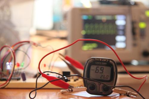
Create a electric shock resistant tool

Youve electric shock?? .. Well, .. it was nice to recover all your gout! Sometimes true .. but we often do not touch circuit accidentally in the work that is still connected with line / grid (pln) .. pissed, wants I think we stepped on the stuff ..! patient first. 


Is there any easy way to avoid electric shock in repair work .. can even avoid the occurrence of ESD, if we deal with electronic goods which are sensitive to ESD (PC motherboards, mobile phones, circuit digital etc). you raft just like this series .. used as supply for the solder, when dealing with components which are sensitive to ESD and touch (CMOS IC). the greater capacity of the transformer Ampere. the greater the (good) power which can be handled. The second transformer is identical / similar.
Read More..

Thursday, October 16, 2014

Build a Digital Stopwatch 0 60sec

Now Build a Digital Stopwatch 0-60sec By using the same circuit of the Digital Stopwatch 0-99sec , we can add an AND gate, and transform the 0 – 99sec stopwatch to a 0 – 60sec stopwatch.We must find a way to control the RESET function of the BCD counter, which is responsible for the counting of the seconds. As we studied above, the circuit resets when we have 99 to 100, that is 1001 1001 à 0001 0000 0000. To make a transformation successfully we must force the pulse from 59 to 60 0011 1001 à 0100 0000 on the output of the BCD counter.

 By placing the AND gate, with its inputs on the Q1 and Q2 of the BCD counter of the decades, we make sure that when the gate closes, the RST input of the BCD counter will be set to logical “1”, which on its turn, will force the circuit to start over. The transformed circuit appears in picture 2.
Read More..

Wednesday, October 15, 2014

Build a 70 Watt OCL Amplifier Circuit Diagram

OCL power amplifier circuit used in the circuit above is the type of power amplifier OCL (Output Capacitor Less) with a power output of 70 Watt. Circuit 70 Watt power amplifier OCL is working on a class AB with symmetrical voltage source of VCC ± 25 volts DC to ± 32 volts DC. OCL power amplifier circuit uses a 70 watt power transistor complementary transistor TIP in 2955 and TIP 3055. 70 watt power amplifier in the circuit can be used to drive the load (4-16 Ohm loudspeaker). Power supply circuit power amplifier can use power supply circuit with current 5A symmetrical. For stereo audio system needs to make a power amplifier OCL circuit tone control + over 2 units.

70 Watt OCL Amplifier Circuit Diagram


Read More..

Build a High And Low Voltage Cut Off With Time Delay Circuit Diagrams

The power line fluctuations and cut-offs cause damages to electrical appliances connected to the line. It is more serious in the case of domestic appliances like fridge and air conditioners. If a fridge is operated on low voltage, excessive current flows through the motor, which heats up, and get damaged.

The under/over voltage protection circuit with time delay presented here is a low cost and reliable circuit for protecting such equipments from damages. Whenever the power line is switched on it gets connected to the appliance only after a delay of a fixed time. If there is hi/low fluctuations beyond sets limits the appliance get disconnected. The system tries to connect the power back after the specific time delay, the delay being counted from the time of disconnection. If the power down time (time for which the voltage is beyond limits) is less than the delay time, the power resumes after the delay: If it is equal or more, then the power resumes directly.

This circuit has been designed, built and evaluated by me to use as a protector for my home refrigerator. This is designed around readily available semi-conductor devices such as standard bipolar medium power NPN transistor (D313/SL100/C1061), an 8-pin type 741 op-amp and NE555 timer IC. Its salient feature is that no relay hunting is employed. This draw back is commonly found in the proctors available in the market.

The complete circuit is consisting of various stages. They are: - Dual rail power supply, Reference voltage source, Voltage comparators for hi/low cut offs, Time delay stage and Relay driver stage. Lets now look at the step-by-step design details.

Dual rail power supply.
This is a conventional type of power supply as shown in Figure 1. The power is applied through the step-down transformer (230/12-0-12V/500mA). The DC proportional to the charging input voltage is obtained from bridge rectifier. Two electrolytics are there to bypass any spikes present. Bridge is capable of handling currents up to 1 Amp.
Output is given by: -
V(out) = 0.71 X V (secondary)
= 0.71 X 24V
= 17.04 V
(This equation is similar for the negative rail as well)

Circuit diagram


Low voltage cut off op-amp
Figure 2 shows the use of very common and easily available op-amp 741 as a comparator. The op-amp is available in TO-5 and DIP type packing.

Circuit diagram


In this ckt the zener diode D1 and it’s associated resistor R1 are connected to the non-inverting terminal (+ve) of 741 to give the suitable reference voltage. The DC voltage from the sensor is given to the inverting (-ve) terminal through pre-set R2.This is used to set the input level.
When the sensor input is less than Zener voltage the output from the Op-amp remains high and when it is greater than Zener voltage the output goes low. When the sensing voltage is equal to Zener voltage the output of the op-amp is approximately zero.
This phenomenon is used as a decision for switching the relay and to give cutoff in a low voltage situation.

High voltage cut off op-amp
Here the op-amp is used as a inverted amplifier. See Figure 3.Zener and resistor network gives reference voltage to the inverting terminal (-ve) of op-amp. Sensing voltage derived through the 10 K pre-set is given to the non- inverting (+ve) terminal and this sets the high level cut.

When the input DC from the sensor is less than Zener voltage the output of the op-amp is low and vice-versa. When the input DC voltage is equal to the zener voltage, the op-amps output is approximately zero.

Circuit diagram


Time delay
I’ve selected the 555 timer due to following reasons.
1. Timing from microseconds through hours.
2. Ability to operate from wide range of supply voltages.
3. High temperature stability.
4. Easily Available.
5. Its triggering circuit is quite sensitive.

This is basically a monostable. The external timing capacitor C2 is held initially discharged by the timer. The circuit triggers upon receiving a pulse to its pin 2 when the level reaches 1/3 Vcc. Once triggered., the circuit will remain in that state until the set time is elapsed or power to the circuit cuts off. The delayed period in seconds is 1.1 C2.R1 where R1 is in megohms and C2 is in microfarads. In practice, R1 should not exceed 20 M. If you use an electrolytic capacitor for C2, select a unit for low leakage. The time delay may have to be adjusted by varying R1 to compensate for the wide tolerance of electrolytics.

Circuit diagram


Relay Driver
The output from the voltage level detectors cannot directly drive the relay and hence the relay driver is used.

Circuit diagram


In this a relay (12V <500 ohms) is connected to the collector of npn transistor. the out put voltage from the comparator is applied to the base of npn transistor through a resistance r1. when the output from the comparator is low the transistor is in off state and the relay is in de-energized state. similarly when the output from the comparator goes high the transistor switches on and the flow of current from the collector to emitter of transistor energizes the relay.

Generally in a relay driver circuit, parallel to the relay coil, a diode or a capacitor is used. This is to eliminate the back e.m.f generated by the relay coil when currents are suddenly broken. Capacitor C1 is connected in parallel to the coil, which filters out the back emf but it, slows down the working of relay.

A better method is to connect two diodes (as shown in the figure 5) that stop the relay – transistor junction swinging more than 600mV above the positive rail or below the zero-volt rail. During normal operation the diodes are reverse biased and have no effect on the performance of circuit. But when back emf is induced, the diodes conduct heavily and absorb all transient voltages. However, I have employed the both methods.
The Complete Circuit

Circuit diagram


Under normal operating conditions i.e. when the input voltage is between maximum and minimum limit the output from the both the comparators are low. The transistor Q1 is OFF and the relay is in de-energized (pole connected to N/C pin) state and the output is obtained.

When the input voltage is below or above the limits set by the pre-sets R8 or R9, the output of the Op-Amps goes either low or high and diodes D1 or D2 would be forward biased depending on the situation. Transistor Q1 switches ON and the flow of current from collector to emitter energizes the relay and the output is cutoff.

A small amount of hystersis has been added via feed back resistors R10 & R11 so that the relay turns on when the level falls to a particular value but does not turn again until it raises a substantial amount above this value. Other wise the relay contacts will frequently turn on/off and produce chattering.

Construction Hints
1) I used a piece of varoboard, which has copper strips on one side to mount the components, and housed the entire circuit and the transformer in a discarded ATX PC power supply box.

2) An autotransformer has been used to set the limits. Set the output of the autotransformer to 250V AC and connect it to the primary of transformer T1 (see Figure 1). Then adjust the pre-set R9 such that relay just energizes. This is the high limit. Next set the output of the autotransformer to 200V AC and adjust the pre-set R8 such that the relay energizes. Please note that these are my preferred limits but you may select any range from say 170 to 270V AC.

3) A neon with a suitable resistor could be connected between the AC supply lines as an ON indicator. Alternatively, LED with a current limiting resistor could be connected between the relay coil so when the relay is energized LED will indicate the situation.
Read More..

Thursday, October 2, 2014

How to Make a Simple FM Radio Circuit

This straightforward fm radio receiver circuit involves a regenerative rf stage, TR1, accompanied by a 2 of three-stage sound amplifier, TR2 to TR4.
In certain spots 3 steps of music boosting most likely are not needed, wherein situation TR3 and its related parts could be excluded as well as the free end of capacitor C5 linked to the collector of TR2.

The crucial portion of the fm radio receiver is the initial stage, TR1/VC1, in which the wirings needs to be kept as tight as they can. Coil L1 is established by winding 8 turns of 1mm (20 swg) enamelled copper wire on a six mm diameter former, that may be in that case eliminated. Following that L1 must be extended cautiously and uniformly to a length of about 13mm.

Transistors List
TR1 = BF199
TR2 = TR3 = TR4 = BC547

The tunning capacitor VC1 is among the 2 fm areas of a tiny fm transistor radio with integrated trimmers (VC2). The “earthy” tail (moving vanes and spindle) is hooked up to the 22pF capacitor C1. The value of the rf choke L2 is not important, whatever from 1µH to 10µH genuinely acceptable.

The output is appropriate for regular headphones linked in series to offer an impedance of 64Ω.

Tuning-in the fm radio receiver

To the radio receiver, potentiometer VR1 should initially be promoted gradually (in the direction of the end of the path linked to battery positive) until, at around the half-way position, an abrupt little rise in background disturbances is going to be heard, suggesting the beginning of oscillation. It after that must be assisted off, extremely steadily, until oscillation simply ceases; it next has to be easy to tweak in a few stations.

The right frequency range of 87 MHz to 108 MHz can be acquired by fine-tuning VC2 at the higher frequency (108 MHz) and somewhat flexing or squeezing jointly the turns of coil L1 towards the end (87 MHz).

About Frequency Modulation

FM transmitting is a transmission know-how pioneered by Edwin Howard Armstrong which employs frequency modulation (FM) to high-fidelity audio over broadcast radio. The "FM band" is the "frequency spectrum wherein FM is utilized for broadcasting". This phrase is moderately inaccurate, because it relates a modulation approach with a variety of frequencies.
Read More..

Thursday, September 18, 2014

Converting a DCM Motor

We recently bought a train set made by a renowned company and just couldn’t resist looking inside the locomotive. Although it did have an electronic decoder, the DCM motor was already available 35 (!) years ago. It is most likely that this motor is used due to financial constraints, because Märklin (as you probably guessed) also has a modern 5-pole motor as part of its range. Incidentally, they have recently introduced a brushless model. The DCM motor used in our locomotive is still an old-fashioned 3-pole series motor with an electromagnet to provide motive power. The new 5-pole motor has a permanent magnet.

We therefore wondered if we couldn’t improve the driving characteristics if we powered the field winding separately, using a bridge rectifier and a 27 Ω current limiting resistor. This would effectively create a permanent magnet. The result was that the driving characteristics improved at lower speeds, but the initial acceleration remained the same. But a constant 0.5 A flows through the winding, which seems wasteful of the (limited) track power. A small circuit can reduce this current to less than half, making this technique more acceptable. The field winding has to be disconnected from the rest (3 wires).

Converting
A freewheeling diode (D1, Schottky) is then connected across the whole winding. The centre tap of the winding is no longer used. When FET T1 turns on, the current through the winding increases from zero until it reaches about 0.5 A. At this current the voltage drop across R4-R7 becomes greater than the reference voltage across D2 and the opamp will turn off the FET. The current through the winding continues flowing via D1, gradually reducing in strength. When the current has fallen about 10% (due to hysteresis caused by R3), IC1 will turn on T1 again. The current will increase again to 0.5 A and the FET is turned off again. This goes on continuously.

The current through the field winding is fairly constant, creating a good imitation of a permanent magnet. The nice thing about this circuit is that the total current consumption is only about 0.2 A, whereas the current flow through the winding is a continuous 0.5 A. We made this modification because we wanted to convert the locomotive for use with a DCC decoder. A new controller is needed in any case, because the polarity on the rotor winding has to be reversed to change its direction of rotation. In the original motor this was done by using the other half of the winding. There is also a good non-electrical alternative: put a permanent magnet in the motor. But we didn’t have a suitable magnet, whereas all electronic parts could be picked straight from the spares box.
 
Read More..

Saturday, September 13, 2014

12 Volt 2 A Switching Power Supply Wiring diagram Schematic

This is a Simple 12 Volt / 2 A Switching Power Supply Circuit Diagram. The schema 12 volt / 2 A switching power supply in the above scheme is not too complicated. At the output of this block provides a stable 12 V and maximum current 2A. Power supply units are quite compact and is suitable for debugging schemes, as well as a permanent resource for stationary devices, including power for the logic electronics for the home-made ​​CNC machine tools.

12 Volt / 2 A Switching Power Supply Circuit Diagram


 12

 Transformer is available in the free market and avoids the hassle of having to self-winding. The diode bridge BR 1 of any given voltage and current of 2A. All other elements in the high part of the schema are designed by the same voltage, taking into account the mains. The scheme of 12 volt / 2 A switching power supply operates from the high voltage network, to be observed when mounting accuracy and caution when using. It is desirable to block the finished board to “pack” in the body.

Sourced By : Circuitsstream
Read More..

Friday, September 12, 2014

LM1758 A Switching Regulator Circuit

The National Semiconductor LM 1578 A is very a switching regulator Which should easily be set up for such dc-to-dc voltage .conversion circuits as the buck, boost, and inverting configurations. The LM 1578 A features a distinctive comparator input stage Which not just} has separate pins for both the inverting and non-inverting inputs, but as well offers an internal 1.0 V reference to every input, thereby simplifying circuit design and PC board layout.

The output can switch upto 750 m A and has output pins for its collector and emitter to market design flexibility. An external current limit terminal tend to be referenced to either the ground or the Vin terminal, depending upon the application. In addition, the LM 1578 A has an on board oscillator, Which sets the switching frequency with other a single external capacitor in one < 1 Hz to 100 kHz (typical). It operates in one supply voltages of 2 V to 40 V. its really provided with other current limit and thermal shutdown. Duty cycle up to 90 %. Functional diagram is given in figure.
Read More..

Friday, September 5, 2014

Schematic diagram of a USB player

Usb series player is an electronic device or electronic circuit that functions as an MP3 player that is stored on a storage device such as USB flash.
In this usb circuit using an IC as a modifier of digital voice data into analog so that it can be applied to a headphone, or again through the power amlplifier strengthened so that it can be heard through the speakers. IC used in this circuit using IC PCM2902 as a modifier of a digital data into analog data storage.


Below is a schematic diagram of a USB player.
USB
Schematic usb player
Read More..

Tuesday, September 2, 2014

Digital Thermometer with data processing of a microcontroller AT89C4051

digital
Digital Thermometer 0-100.0°C is a digital thermometer that operates in modetemperature measurement in Celsius (° C). Digital Thermometer 0-100.0 ° C in this article uses data processor in the form of a microcontroller AT89C4051.


Temperature sensors used in Digital Thermometer 0-100.0 ° C. This temperature sensor LM35D. Digital Thermometer 0-100.0 ° C. It uses the temperature measurement data viewer in the form of 1 line LCD viewer. Digital Thermometer 0-100.0 ° C. It can display the temperature measurement data with a resolution of 0.1 ° C.

Digital
Digital Thermometer Circuit Diagram


Digital Thermometer 0-100.0 ° C. These temperature sensors make use of LM35D as temperature sensing. In Digital Thermometer 0-100.0 ° C. This temperature sensor measurement data this LM35D (Level Voltage) is then converted into 4-bit binary data using the ADC CA3162.

Then the 4-bit data from ADC CA3162 which is a measurement of data if the temperature is in the AT89C4951 microcontroller so that it becomes an operating principle of temperature measurement based on digital thermometers. In the final stage of the Digital Thermometer 0-100.0 ° C. This is the appearance of digital data temperature measurement, using digital data viewer of the LCD 1 line.
Read More..

Monday, September 1, 2014

Build a CW Signal Processor Wiring diagram Schematic

How to Build a CW Signal Processor Circuit Diagram? That is a good question but i explain this way. This schema provides interferenced rejection for the CW operator. The 567 phase-locked loop is configured to respond to tones from 500 to 1100 Hz. The Schmitt trigger reduces the weighting effect caused by the output of the PLL remaining low after removal of the audio signal. 

Ten to 15 millivolts of audio activate the schema. For periods of loss of signal, schema B will automatically switch back to live receiver audio after a suitable delay. (If a relay with a 5-volt coil is not available, the schema can also be powered from +12 volts) When schema B is used, the contacts on relay K1 replace SI.

CW Signal Processor Circuit Diagram

Build

Read More..

Saturday, August 30, 2014

Save Your Ears A Noise Meter

‘Hello… HELLO! Are you deaf? Do you have disco ears?’ If people ask you this and you’re still well below 80 , you may be suffering from hearing loss, which can come from (prolonged) listening to very loud music. You won’t notice how bad it is until it’s too late, and after that you won’t be able to hear your favorite music the way it really is – so an expensive sound system is no longer a sound investment. To avoid all this, use the i-trixx sound meter to save your ears (and your neighbors ears!).
With just a handful of components, you can build a simple but effective sound level meter for your sound system. This sort of schema is also called a VU meter. The abbreviation ‘VU’ stands for ‘volume unit’, which is used to express the average value of a music signal over a short time. The VU meter described here is what is called a ‘passive’ type. This means it does not need a separate power supply, since the power is provided by the input signal. This makes it easy to use: just connect it to the loudspeaker terminals (the polarity doesn’t matter) and you’re all set.
The more LEDs that light up while the music is playing, the more you should be asking yourself how well you are treating your ears (and your neighbours’ ears). Of course, this isn’t an accurately calibrated meter. The schema design is too simple (and too inexpensive) for that. However, you can have a non-disco type (or your neighbors) tell you when the music is really too loud, and the maximum number of LED lit up at that time can serve you as a good reference for the maximum tolerable sound level.
Although this is a passive VU meter, it contains active components in the form of two transistors and six FETs. Seven LEDs light up in steps to show how much power is being pumped into the loudspeaker. The steps correspond to the power levels shown in the schematic for a sine-wave signal into an 8-ohm load. LED D1 lights up fi rst at low loudspeaker voltages. As the music power increases, the following LEDs (D2, D3, and so on) light up as well. The LEDs thus dance to the rhythm of the music (especially the bass notes).
Circuit diagram:
noise Noise Meter Circuit Diagram
This schema can easily be assembled on a small piece of prototyping board. Use low-current types for the LEDs. They have a low forward voltage and are fairly bright at current levels as low as 1 mA. Connect the VU meter to the loudspeaker you want to monitor. If LED D2 never lights up (it remains dark even when LED D3 lights up), reverse the polarity of diode D8 (we have more to say about this later on). In addition, bear in mind that the sound from the speaker will have to be fairly loud before the LEDs will start lighting up.
If you want to know more about the technical details this VU meter, keep on reading. Each LED is driven by its own current source so it will not be overloaded with too much current when the input voltage increases. The current sources also ensure that the final amplifier is not loaded any more than necessary. The current sources for LEDs D1–D6 are formed by FET diagram. A FET can be made to supply a fixed current by simply connecting a resistor to the source lead (resistors R1–R6 in this case). With a resistance of 1 kΩ, the current is theoretically limited to 1 mA. However, in practice FETs have a especially broad tolerance range. The actual current level with our prototype ranged from 0.65 mA to 0.98 mA.
To ensure that each LED only lights up starting at a defined voltage, a Zener diode (D8–D13) is connected in series with each LED starting with D2. The Zener voltage must be approximately 3 V less than the voltage necessary for the indicated power level. The 3-V offset is a consequence of the voltage losses resulting from the LED, the FET, the rectifier, and the over voltage protection. The over voltage protection is combined with the current source for LED D7. One problem with using FETs as current sources is that the maximum rated drain–source voltage of the types used here is only 30 V.
If you want to use the schema with an especially powerful fi nal amplifier, a maximum input level of slightly more than 30 V is much too low. We thus decided to double the limit. This job is handled by T7 and T8. If the amplitude of the applied signal is less than 30 V, T8 buffers the rectified voltage on C1. This means that when only the first LED is lit, the additional voltage drop of the over voltage protection schema is primarily determined by the base–emitter voltage of T8. The maximum worst-case voltage drop across R8 is 0.7 V when all the LEDs are on, but it has increasingly less effect as the input voltage rises.
R8 is necessary so the base voltage can be regulated. R7 is fitted in series with LED D7 and Zener diode D13, and the voltage drop across R7 is used to cause transistor T7 to conduct. This voltage may be around 0.3 V at very low current levels, but with a current of a few mili-amperes it can be assumed to be 0.6 V. Transistor T7 starts conducting if the input voltage rises above the threshold voltage of D7 and D13, and this reduces the voltage on the base of T8. This negative feedback stabilizes the supply voltage for the LEDs at a level of around 30 V. With a value of 390 Ω for R7, the current through LED D7 will be slightly more than 1 mA.
This has been done intentionally so D7 will be a bit brighter than the other LEDs when the signal level is above 30 V. When the voltage is higher than 30 V, the schema draws additional current due to the voltage drop across R8. The AC voltage on the loudspeaker terminals is half-wave rectifi ed by diode D14. This standard diode can handle 1 A at 400 V. The peak current level can be considerably higher, but don’t forget that the current still has to be provided by the fi nal amplifier.
Resistor R9 is included in series with the input to keep the additional load on the fi nal amplifi er within safe bounds and limit the interference or distortion that may result from this load. The peak current can never exceed 1.5 A (the charging current of C1), even when the schema is connected directly to an AC voltage with an amplitude of 60 V. C1 also determines how long the LEDs stay lit. This brings us to an important aspect of the schema, which you may wish to experiment with in combination with the current through the LEDs.
An important consideration in the schema design is to keep the load on the fi nal amplifi er to a minimum. However, the combination of R9 and C1 causes an averaging of the complex music signal. The peak signal levels in the music are higher (or even much higher) than the average value. Tests made under actual conditions show that the applied peak power can easily be a factor of 2 to 4 greater than what is indicated by this VU meter. This amounts to 240 W or more with an 8-Ω loudspeaker.
You can reduce the value of C1 to make the schema respond more quickly (and thus more accurately) to peak signal levels. Now a few comments on D8. You may receive a stabistor (for example, from the Philips BZV86 series or the like) for D8. Unlike a Zener diode, a stabistor must be connected in the forward-biased direction. A stabistor actually consists of a set of PN junctions in series (or ordinary forward-biased diodes). Check this carefully: if D2 does not light up when D8 is fi tted as a normal Zener diode, then D8 quite likely a stabistor, so you should fi t it the other way round.
Read More..

Wednesday, August 20, 2014

Build a Variable 5 to 20V DC Supply Wiring diagram Schematic

This is a Variable 5 to 20V DC Supply Circuit Diagram. If you are looking for a low drop voltage regulator that can provide a power supply of 1A with an output voltage of between 5V and 20V DC, National Semiconductor LM2941 Low Dropout Adjustable Regulator is that you can pick to make use of. Its a typical dropout voltage of 0.5V which means that the input supply need only must be 0.5V DC over the desired output voltage. 

Variable 5 to 20V DC Supply Circuit Diagram

Variable
 
Its other features include internal short schema current limit and reverse battery protection. As shown in the schematic below, the regulator has five pins which consists of the ON/OFF control, Input Voltage, Output Voltage, Ground & Adjustable pins. ON/OFF is used for the purpose of switching on & off of the regulator. The capacitors C1 & E1 are to be placed as close as feasible to the regulator. 

The output of the schema can be varied by varying the worth of potentiometer VR1 from 5V DC to 20V DC. The input voltage is limited from five.5V DC to 30V DC. Resistor R1 must be greater than 1K. The worth of the VR1 that needs to be set is calculated from the formula given below: 

VR1 = R1[(Vout/1.275) - 1] ohm
 If R1=1K, Vout = 5V, VR1 should be set to 2.9K ohm. 
 If R1=1K, Vout = 20V, VR1 should be set to 14.7K ohm


Read More..

Monday, August 18, 2014

Build a Bipolar Power supply for Battery instruments

How to Build a Bipolar Power supply for Battery instruments. A bipolar power supply overcomes those limitations. Most importantly, it can provide both positive and negative voltages from a single pair of terminals. There are no relays to switch polarity, so a bipolar supply can move smoothly from positive, through zero, to negative voltages. 

 Bipolar Power supply for Battery instruments Circuit Diagram

Bipolar

It also regulates zero volts or other very small voltages. In this Bipolar Power supply for Battery instruments schema diagram to generate regulated ± 5-V supplies from a pair of dry batteries, the schema of Fig. 1 is commonly used. In order to give protection from inadvertent reverse connection of a battery, a diode in series with each battery would produce an unacceptable voltage drop. 

The more effective approach is to fit diodes Dl and D2 as shown in Fig. 2, in parallel with each battery. When the supply is switched off, there is the risk of a reverse bias being applied across the regulators, if there is significant inductance or capacitance in the load schema. Diodes across the regulators prevent damage. When the power supply is switched on, the two switches do not act in unison. 

There is a probability that one or the other regulators will be latched hard off by the other. To prevent this, D3 and D4 are Zener diodes so that ± 5-V rails are pulled up by the batteries until the regulators establish the correct levels.
Read More..

Sunday, August 17, 2014

Build a 9V Wireless Microphone FM Transmitter

This FM transmitter schema can be used as a wireless microphone,  can be received by an ordinary 88- to 108-MHz FM broadcast receiver. For the power supply, this transmitter schema is powered by a 9 V battery. To comply with the radiation limit of FCC rules, keep the antenna length under 12 inches. L1 is 6 turns of #24 wire wound around a pencil or a 1/4″ form, with turns spacing of 1 wire diameter. C6 is a gimmick capacitor which has value about 1 pF.

 9V Wireless Microphone FM Transmitter Circuit Diagram


Build

Read More..

Saturday, August 16, 2014

Track Your Distance Through a Bicycle Odometer

Just like cars that measures the distance it can travel, you can also do it with your bicycles. We usually keep track of our mileage to see how far our strength can go but would it be of great use if we track it because we are maintaining a workout everyday considering the calories we are burning.

Hacks and Mods: Track Your Distance Through a Bicycle Odometer

If you want to make your own odometer, you will need a micro controller that generates pulse and a MOSFET that converts those voltage pulses. Just remember to check your batteries all the time.
The best way of burning calories is to move those muscles everyday! Set your bikes and your odometer! Burn fats!

Read More..

A Car Battery Monitor

A close call on the road can really focus your mind on the importance of having a battery monitor in a car. I had been enjoying a pleasant week of travelling around the countryside at a leisurely pace and taking in the beautiful scenery each day. It wasnt until the final day, with the big rush to return home, that I had to drive at night.My home is deep in the country and on the road I was travelling the closest petrol station may be 80km away. I was travelling through an area that is full of open-cut coal mines and large heavily loaded semi-trailers constantly pound the roads, travelling at quite high speeds. It was around 8pm at night and everything was very dark no street lights or house lights anywhere.

Just as I was going up a hill, the lights began to dim and the engine coughed. A large semi-trailer loomed in the rear-vision mirror as I pushed the clutch in and tried to restart. My speed was falling rapidly and my lights were blacked out - I was like a sitting duck in the middle of the road, as the semi-trailer came rapidly bearing down on me. I just managed to pull the car off the road, as the semi-trailer came screaming past, missing me by inches! After calling for assistance from the NRMA, the problem was found to be a fault in the alternator, which was failing to charge the battery. The battery voltage had been falling under the heavy load of the lights and at the worst possible time, there was not sufficient power for the lights or the motor.

 A Car Battery Monitor Circuit Diagram

 A Car Battery Monitor Circuit Diagram


After the initial shock wore off, I put on my thinking cap to come up with a PIC-based solution to the problem. What was really needed was a display and a buzzer, to get my attention should the voltage fall outside a specified range. So my design criteria was set, a series of LEDs could indicate the voltage and a buzzer would also be used to warn of problems.
Main Features:
  • Visual indication of battery voltage
  • Audible warning when voltage becomes low
  • Screw terminals for easy connection
  • Simple and easy to build
Circuit details:

The schema is based on PIC16F819 18-pin microcontroller which has an analog-to-digital (A/D) input to monitor the battery voltage and outputs capable of driving LEDs directly, to keep the component count down. There are seven LEDs in all, giving a good range of voltage indication. The topmost LED, LED1, comes on for voltages above 14V which will occur when the battery is fully charged. LED2 indicates for voltages between 13.5V and 14V while LED3 indicates between 13V and 13.5V. Normally, one of these LEDs will be on. LED4 covers 12.5V to 13V while LED5 covers 12V to 12.5V. LED6 covers from 11.5V to 12V while LED7 comes on for voltages below 11.5V. These two LEDs are backed up by the piezo chime which beeps for voltages between 11.5V and 12V and becomes more insistent for voltages below 11.5V.

That might seem fairly conservative. After all, most cars will start with no troubles, even though the battery voltage might be a touch below 12V, wont they? Well, no. Some modern cars will happily crank the motor at voltages below 11V but their engine management will not let the motor start unless the voltage is above 11V. So dont think that a modern car will always start reliably. This little battery monitor could easily prevent a very inconvenient failure to start! So lets describe the rest of the schema. The incoming supply is connected via diode D1 which provides protection against reverse polarity while zener diode ZD1 provides protection from spike voltages.

A standard 7805 3-terminal regulator is then used to provide a stable 5V to the microcontroller. The battery voltage is sensed via a voltage divider using 33kΩ and 100kΩ resistors. This brings the voltage down to within the 0-5V range for the A/D input of the PIC16F819. Port B (RB0 to RB7) of the microcontroller is then used to drive the various LEDs, with current limiting provided via the 330Ω resistor network. RB7, pin 13, drives a switching transistor for the piezo buzzer.

Software:
For the software, the design follows the basic template for a PIC microcontroller. Port A and its ADC (analog-to-digital converter) function are set up while port B functions as the output for the LEDs and buzzer. Once the set-up is complete, a reading will be taken at port RA2, the input for the A/D convertor. This reading is then compared with a series of values to determine the range of the voltage. This is similar to a series of "if" statements in Basic language. If the voltage is found to be within a certain range, the relevant port B pin will be turned on. If the voltage is below 12V, the buzzer will be turned on for a brief period, to signal a low battery condition. As the voltage falls below 11.5V, the frequency of the beeps will increase, to signal increased urgency.

Building it:

All the parts are mounted on a small PC board measuring 46 x 46mm (available from Futurlec). The starting point should be the IC socket for the PIC16F819, as this is easiest to mount while the board is bare. The next item can be the PC terminal block. The resistors and capacitors can then follow. Make sure the electrolytics are inserted with correct polarity.


Make sure that you do not confuse the zener (ZD1) with the diode when you are installing them; the diode is the larger package of the two.
Even more important, dont get the 78L05 3-terminal regulator and the 2N3906 transistor mixed up; they come in identical packages. The 78L05 will be labelled as such while the 2N3906 will be labelled "3906". And make sure you insert them the correct way around. The buzzer must also be installed with the correct polarity. The 330Ω current limiting resistors are all in a 10-pin in-line package. There are four green LEDs, two yellow and one red. They need to be installed in line and with the correct orientation.

Testing:

Before you insert the PIC16F819 microcontroller, do a voltage check. Connect a 12V source and check for the presence of 5V between pins 14 & 5 OF IC1. If 5V is not present, check the polarity of regulator REG1 and the polarity of the diode D1. If these tests are OK, insert the IC and test the unit over a range of voltage between 9V and 15V. Make sure that all LEDs come on in sequence and the piezo buzzer beeps for voltages below 12V. 

Now it is matter of installing the unit in your car. It is preferable to install the unit in a visible position for the driver. However, it should not obscure any other instruments. The unit should be connected to the cars 12V supply after the ignition switch. This will turn the unit off with the other instruments and prevent battery drain while the motor is not running.


Author :Alan Bonnard Copyright : Silicon Chip Publications Pty Ltd
Read More..

Friday, August 15, 2014

Build a 3 Watt Stereo Amplifier Wiring diagram Schematic

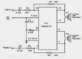
Build a 3 Watt Stereo Amplifier Circuit Diagram. This schema using MAX 7910 IC. The MAX9710 a stereo audio power amplifier IC capable of delivering 3Watts of out put to 4 Ohm loads. MAX9710 can be operated from a single 4.5V to 5.5V power supply , makes it ideal for hand held applications.The IC for 
3 Watt stereo amplifier schema also features thermal overload protection.
 3 Watt Stereo Amplifier Circuit Diagram
3 Watt Stereo Amplifier Circuit Diagram
 This 3 Watt stereo amplifier schema is suitable for small power audio devices such as radio sets and portable CD players. 5 V DC power supply is used for powering the 3 Watt stereo amplifier schema. 6V battery with an IN 4007 diode series to the positive terminal of it can also be used instead of 5 V DC supply. The 3 Watt stereo amplifier schema will get a supply voltage approximately 5 V after 0.7 V voltage drop across diode.
Read More..

Using LED as a diode Rectifier Wiring diagram Schematic

This is a simple LED as a diode Rectifier Circuit Diagram. In certain situations where the current is not high, we can use the famous LED (LED) and diode rectifier voltage power diagram. The LED can be used without problem in a rectification schema, and also works in the power ratings. Pay attention not to exceed the maximum current of the LED in a wave rectifier.


 Using LED as a diode Rectifier Circuit Diagram

Using LED as a diode Rectifier Circuit Diagram

Read More..

Thursday, August 14, 2014

Build a Room Ioniser Wiring diagram Schematic

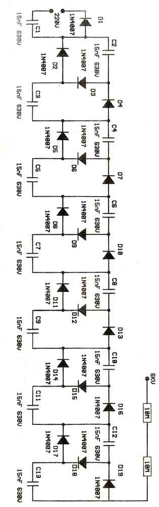
This is a voltage multiplier schema acting as an Room Ioniser Circuit Diagram. Its calculated to feed 220V from mains and the output is about 6KV. Caution should take with the schema as can be dangerous due to mains. You can place a needle at the output 3cm long. Even you disconnect from mains, capacitors can be dangerous so make sure to discharge them by shorting their pins before you touch the schema with hands.

Room Ioniser Circuit Diagram

Build a Room Ioniser Circuit Diagram
 
Read More..