Showing posts with label build. Show all posts
Showing posts with label build. Show all posts
Thursday, October 16, 2014
Build a Digital Stopwatch 0 60sec
Now Build a Digital Stopwatch 0-60sec By using the same circuit of the Digital Stopwatch 0-99sec , we can add an AND gate, and transform the 0 – 99sec stopwatch to a 0 – 60sec stopwatch.We must find a way to control the RESET function of the BCD counter, which is responsible for the counting of the seconds. As we studied above, the circuit resets when we have 99 to 100, that is 1001 1001 à 0001 0000 0000. To make a transformation successfully we must force the pulse from 59 to 60 0011 1001 à 0100 0000 on the output of the BCD counter.

By placing the AND gate, with its inputs on the Q1 and Q2 of the BCD counter of the decades, we make sure that when the gate closes, the RST input of the BCD counter will be set to logical “1”, which on its turn, will force the circuit to start over. The transformed circuit appears in picture 2.

Wednesday, October 15, 2014
Build a 70 Watt OCL Amplifier Circuit Diagram
OCL power amplifier circuit used in the circuit above is the type of power amplifier OCL (Output Capacitor Less) with a power output of 70 Watt. Circuit 70 Watt power amplifier OCL is working on a class AB with symmetrical voltage source of VCC ± 25 volts DC to ± 32 volts DC. OCL power amplifier circuit uses a 70 watt power transistor complementary transistor TIP in 2955 and TIP 3055. 70 watt power amplifier in the circuit can be used to drive the load (4-16 Ohm loudspeaker). Power supply circuit power amplifier can use power supply circuit with current 5A symmetrical. For stereo audio system needs to make a power amplifier OCL circuit tone control + over 2 units.
70 Watt OCL Amplifier Circuit Diagram

70 Watt OCL Amplifier Circuit Diagram

Build a High And Low Voltage Cut Off With Time Delay Circuit Diagrams
The power line fluctuations and cut-offs cause damages to electrical appliances connected to the line. It is more serious in the case of domestic appliances like fridge and air conditioners. If a fridge is operated on low voltage, excessive current flows through the motor, which heats up, and get damaged.
The under/over voltage protection circuit with time delay presented here is a low cost and reliable circuit for protecting such equipments from damages. Whenever the power line is switched on it gets connected to the appliance only after a delay of a fixed time. If there is hi/low fluctuations beyond sets limits the appliance get disconnected. The system tries to connect the power back after the specific time delay, the delay being counted from the time of disconnection. If the power down time (time for which the voltage is beyond limits) is less than the delay time, the power resumes after the delay: If it is equal or more, then the power resumes directly.
This circuit has been designed, built and evaluated by me to use as a protector for my home refrigerator. This is designed around readily available semi-conductor devices such as standard bipolar medium power NPN transistor (D313/SL100/C1061), an 8-pin type 741 op-amp and NE555 timer IC. Its salient feature is that no relay hunting is employed. This draw back is commonly found in the proctors available in the market.
The complete circuit is consisting of various stages. They are: - Dual rail power supply, Reference voltage source, Voltage comparators for hi/low cut offs, Time delay stage and Relay driver stage. Lets now look at the step-by-step design details.
Dual rail power supply.
This is a conventional type of power supply as shown in Figure 1. The power is applied through the step-down transformer (230/12-0-12V/500mA). The DC proportional to the charging input voltage is obtained from bridge rectifier. Two electrolytics are there to bypass any spikes present. Bridge is capable of handling currents up to 1 Amp.
Output is given by: -
V(out) = 0.71 X V (secondary)
= 0.71 X 24V
= 17.04 V
(This equation is similar for the negative rail as well)
This is a conventional type of power supply as shown in Figure 1. The power is applied through the step-down transformer (230/12-0-12V/500mA). The DC proportional to the charging input voltage is obtained from bridge rectifier. Two electrolytics are there to bypass any spikes present. Bridge is capable of handling currents up to 1 Amp.
Output is given by: -
V(out) = 0.71 X V (secondary)
= 0.71 X 24V
= 17.04 V
(This equation is similar for the negative rail as well)
Circuit diagram

Low voltage cut off op-amp
Figure 2 shows the use of very common and easily available op-amp 741 as a comparator. The op-amp is available in TO-5 and DIP type packing.
Figure 2 shows the use of very common and easily available op-amp 741 as a comparator. The op-amp is available in TO-5 and DIP type packing.
Circuit diagram

In this ckt the zener diode D1 and it’s associated resistor R1 are connected to the non-inverting terminal (+ve) of 741 to give the suitable reference voltage. The DC voltage from the sensor is given to the inverting (-ve) terminal through pre-set R2.This is used to set the input level.
When the sensor input is less than Zener voltage the output from the Op-amp remains high and when it is greater than Zener voltage the output goes low. When the sensing voltage is equal to Zener voltage the output of the op-amp is approximately zero.
This phenomenon is used as a decision for switching the relay and to give cutoff in a low voltage situation.
When the sensor input is less than Zener voltage the output from the Op-amp remains high and when it is greater than Zener voltage the output goes low. When the sensing voltage is equal to Zener voltage the output of the op-amp is approximately zero.
This phenomenon is used as a decision for switching the relay and to give cutoff in a low voltage situation.
High voltage cut off op-amp
Here the op-amp is used as a inverted amplifier. See Figure 3.Zener and resistor network gives reference voltage to the inverting terminal (-ve) of op-amp. Sensing voltage derived through the 10 K pre-set is given to the non- inverting (+ve) terminal and this sets the high level cut.
Here the op-amp is used as a inverted amplifier. See Figure 3.Zener and resistor network gives reference voltage to the inverting terminal (-ve) of op-amp. Sensing voltage derived through the 10 K pre-set is given to the non- inverting (+ve) terminal and this sets the high level cut.
When the input DC from the sensor is less than Zener voltage the output of the op-amp is low and vice-versa. When the input DC voltage is equal to the zener voltage, the op-amps output is approximately zero.
Circuit diagram

Time delay
I’ve selected the 555 timer due to following reasons.
1. Timing from microseconds through hours.
2. Ability to operate from wide range of supply voltages.
3. High temperature stability.
4. Easily Available.
5. Its triggering circuit is quite sensitive.
I’ve selected the 555 timer due to following reasons.
1. Timing from microseconds through hours.
2. Ability to operate from wide range of supply voltages.
3. High temperature stability.
4. Easily Available.
5. Its triggering circuit is quite sensitive.
This is basically a monostable. The external timing capacitor C2 is held initially discharged by the timer. The circuit triggers upon receiving a pulse to its pin 2 when the level reaches 1/3 Vcc. Once triggered., the circuit will remain in that state until the set time is elapsed or power to the circuit cuts off. The delayed period in seconds is 1.1 C2.R1 where R1 is in megohms and C2 is in microfarads. In practice, R1 should not exceed 20 M. If you use an electrolytic capacitor for C2, select a unit for low leakage. The time delay may have to be adjusted by varying R1 to compensate for the wide tolerance of electrolytics.
Circuit diagram

Relay Driver
The output from the voltage level detectors cannot directly drive the relay and hence the relay driver is used.
The output from the voltage level detectors cannot directly drive the relay and hence the relay driver is used.
Circuit diagram

In this a relay (12V <500 ohms) is connected to the collector of npn transistor. the out put voltage from the comparator is applied to the base of npn transistor through a resistance r1. when the output from the comparator is low the transistor is in off state and the relay is in de-energized state. similarly when the output from the comparator goes high the transistor switches on and the flow of current from the collector to emitter of transistor energizes the relay.
Generally in a relay driver circuit, parallel to the relay coil, a diode or a capacitor is used. This is to eliminate the back e.m.f generated by the relay coil when currents are suddenly broken. Capacitor C1 is connected in parallel to the coil, which filters out the back emf but it, slows down the working of relay.
A better method is to connect two diodes (as shown in the figure 5) that stop the relay – transistor junction swinging more than 600mV above the positive rail or below the zero-volt rail. During normal operation the diodes are reverse biased and have no effect on the performance of circuit. But when back emf is induced, the diodes conduct heavily and absorb all transient voltages. However, I have employed the both methods.
The Complete Circuit
Circuit diagram

Under normal operating conditions i.e. when the input voltage is between maximum and minimum limit the output from the both the comparators are low. The transistor Q1 is OFF and the relay is in de-energized (pole connected to N/C pin) state and the output is obtained.
When the input voltage is below or above the limits set by the pre-sets R8 or R9, the output of the Op-Amps goes either low or high and diodes D1 or D2 would be forward biased depending on the situation. Transistor Q1 switches ON and the flow of current from collector to emitter energizes the relay and the output is cutoff.
A small amount of hystersis has been added via feed back resistors R10 & R11 so that the relay turns on when the level falls to a particular value but does not turn again until it raises a substantial amount above this value. Other wise the relay contacts will frequently turn on/off and produce chattering.
Construction Hints
1) I used a piece of varoboard, which has copper strips on one side to mount the components, and housed the entire circuit and the transformer in a discarded ATX PC power supply box.
1) I used a piece of varoboard, which has copper strips on one side to mount the components, and housed the entire circuit and the transformer in a discarded ATX PC power supply box.
2) An autotransformer has been used to set the limits. Set the output of the autotransformer to 250V AC and connect it to the primary of transformer T1 (see Figure 1). Then adjust the pre-set R9 such that relay just energizes. This is the high limit. Next set the output of the autotransformer to 200V AC and adjust the pre-set R8 such that the relay energizes. Please note that these are my preferred limits but you may select any range from say 170 to 270V AC.
3) A neon with a suitable resistor could be connected between the AC supply lines as an ON indicator. Alternatively, LED with a current limiting resistor could be connected between the relay coil so when the relay is energized LED will indicate the situation.
Monday, September 1, 2014
Build a CW Signal Processor Wiring diagram Schematic
How to Build a CW Signal Processor Circuit Diagram? That is a good question but i explain this way. This schema provides interferenced rejection for the CW operator. The 567 phase-locked loop is configured to respond to tones from 500 to 1100 Hz. The Schmitt trigger reduces the weighting effect caused by the output of the PLL remaining low after removal of the audio signal.
Ten to 15 millivolts of audio activate the schema. For periods of loss of signal, schema B will automatically switch back to live receiver audio after a suitable delay. (If a relay with a 5-volt coil is not available, the schema can also be powered from +12 volts) When schema B is used, the contacts on relay K1 replace SI.
CW Signal Processor Circuit Diagram
Wednesday, August 20, 2014
Build a Variable 5 to 20V DC Supply Wiring diagram Schematic
This is a Variable 5 to 20V DC Supply Circuit Diagram. If you are looking for a low drop voltage regulator that can provide a power supply of 1A with an output voltage of between 5V and 20V DC, National Semiconductor LM2941 Low Dropout Adjustable Regulator is that you can pick to make use of. Its a typical dropout voltage of 0.5V which means that the input supply need only must be 0.5V DC over the desired output voltage.
Variable 5 to 20V DC Supply Circuit Diagram
Its other features include internal short schema current limit and reverse battery protection. As shown in the schematic below, the regulator has five pins which consists of the ON/OFF control, Input Voltage, Output Voltage, Ground & Adjustable pins. ON/OFF is used for the purpose of switching on & off of the regulator. The capacitors C1 & E1 are to be placed as close as feasible to the regulator.
The output of the schema can be varied by varying the worth of potentiometer VR1 from 5V DC to 20V DC. The input voltage is limited from five.5V DC to 30V DC. Resistor R1 must be greater than 1K. The worth of the VR1 that needs to be set is calculated from the formula given below:
VR1 = R1[(Vout/1.275) - 1] ohm
If R1=1K, Vout = 5V, VR1 should be set to 2.9K ohm.
If R1=1K, Vout = 20V, VR1 should be set to 14.7K ohm

Monday, August 18, 2014
Build a Bipolar Power supply for Battery instruments
How to Build a Bipolar Power supply for Battery instruments. A bipolar power supply overcomes those limitations. Most importantly, it can provide both positive and negative voltages from a single pair of terminals. There are no relays to switch polarity, so a bipolar supply can move smoothly from positive, through zero, to negative voltages.
Bipolar Power supply for Battery instruments Circuit Diagram
It also regulates zero volts or other very small voltages. In this Bipolar Power supply for Battery instruments schema diagram to generate regulated ± 5-V supplies from a pair of dry batteries, the schema of Fig. 1 is commonly used. In order to give protection from inadvertent reverse connection of a battery, a diode in series with each battery would produce an unacceptable voltage drop.
The more effective approach is to fit diodes Dl and D2 as shown in Fig. 2, in parallel with each battery. When the supply is switched off, there is the risk of a reverse bias being applied across the regulators, if there is significant inductance or capacitance in the load schema. Diodes across the regulators prevent damage. When the power supply is switched on, the two switches do not act in unison.
There is a probability that one or the other regulators will be latched hard off by the other. To prevent this, D3 and D4 are Zener diodes so that ± 5-V rails are pulled up by the batteries until the regulators establish the correct levels.
Sunday, August 17, 2014
Build a 9V Wireless Microphone FM Transmitter
This FM transmitter schema can be used as a wireless microphone, can be received by an ordinary 88- to 108-MHz FM broadcast receiver. For the power supply, this transmitter schema is powered by a 9 V battery. To comply with the radiation limit of FCC rules, keep the antenna length under 12 inches. L1 is 6 turns of #24 wire wound around a pencil or a 1/4″ form, with turns spacing of 1 wire diameter. C6 is a gimmick capacitor which has value about 1 pF.
9V Wireless Microphone FM Transmitter Circuit Diagram
Friday, August 15, 2014
Build a 3 Watt Stereo Amplifier Wiring diagram Schematic
Build a 3 Watt Stereo Amplifier Circuit Diagram. This schema using MAX 7910 IC. The MAX9710 a stereo audio power amplifier IC capable of delivering 3Watts of out put to 4 Ohm loads. MAX9710 can be operated from a single 4.5V to 5.5V power supply , makes it ideal for hand held applications.The IC for
3 Watt stereo amplifier schema also features thermal overload protection.
3 Watt Stereo Amplifier Circuit Diagram
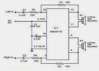
This 3 Watt stereo amplifier schema is suitable for small power audio devices such as radio sets and portable CD players. 5 V DC power supply is used for powering the 3 Watt stereo amplifier schema. 6V battery with an IN 4007 diode series to the positive terminal of it can also be used instead of 5 V DC supply. The 3 Watt stereo amplifier schema will get a supply voltage approximately 5 V after 0.7 V voltage drop across diode.
Thursday, August 14, 2014
Build a Room Ioniser Wiring diagram Schematic
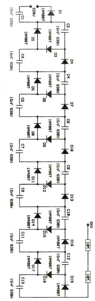
This is a voltage multiplier schema acting as an Room Ioniser Circuit Diagram. Its calculated to feed 220V from mains and the output is about 6KV. Caution should take with the schema as can be dangerous due to mains. You can place a needle at the output 3cm long. Even you disconnect from mains, capacitors can be dangerous so make sure to discharge them by shorting their pins before you touch the schema with hands.
Room Ioniser Circuit Diagram
Build a High voltage Inverter Wiring diagram Schematic
This is a simple High voltage inverter schema diagram. This inverter schema works with a transistor and transformer and other components to increase the voltage becomes high. Input supply voltage ranging from 3V to 6V DC, later it was raised to high voltage AC. However, in this inverter schema output current is very small, probably under 0.1A even smaller. However, its use you can apply it on a fluorescent lamp 10W maximum power only, and that too takes time to switch on fluorescent lamps.
High voltage inverter schema diagram

Part List
R1 = 4K7
R2 = 2K2
R3 = 330K
C1 = 100nF
C2 = 100nF 275V
C3 = 0.22uF 275V
Q1 = D506
L1 = 100 times winding, with 0.8mm diameter copper wire
L2 = 50 times winding, with 0.8mm diameter copper wire
L3 = 5000 times winding, with 0.4mm diameter copper wire
Wednesday, August 13, 2014
Build a Varying Brightness AC Lamp Circuit
Varying Brightness AC Lamp Circuit, an SCR is used to slowly vary the intensity of a 120 volt light bulb by controlling the time that the AC line voltage is applied to the lamp during each half cycle.
Varying Brightness AC Lamp Circuit Diagram

Caution:
The schema is directly connected to the AC power line and should be placed inside an enclosure that will prevent direct contact with any of the components. To avoid electrical shock, do not touch any part of the schema while it is connected to the AC power line. A 2K, 10 watt power resistor is used to drop the line voltage down to 9 volts DC. This resistor will dissipate about 7 watts and needs some ventilation.
Operation:
A couple NPN transistors are used to detect the beginning of each half cycle and trigger a delay timer which in turn triggers the SCR at the end of the delay time. The delay time is established by a current source which is controlled by a 4017 decade counter. The first count (pin 3) sets the current to a minimum which corresponds to about 7 milliseconds of delay, or most of the half cycle time so that the lamp is almost off. Full brightness is obtained on the sixth count (pin 1) which is not connected so that the current will be maximum and provide a minimum delay and trigger the SCR near the beginning of the cycle. The remaining 8 counts increment the brightness 4 steps up and 4 steps down between maximum and minimum. Each step up or down provides about twice or half the power, so that the intensity appears to change linearly. The brightness of each step can be adjusted with the 4 resistors (4.3K, 4.7K, 5.6K, 7.5K) connected to the counter outputs.
The schema has been built by Don Warkentien (WODEW) who suggsted adding a small 47uF capacitor from ground to the junction of the current source transistor (PNP) to reduce the digital stepping effect so the lamp will brighten and fade in a smoother fashion. The value of this capacitor will depend on the 4017 counting rate, a faster rate would require a smaller capacitor.
Sunday, August 10, 2014
Build a Simple 90Vrms Voltage Regulator Circuits Wiring diagram
This is a Simple 90Vrms Voltage Regulator Circuits Diagram. The 90Vrms Voltage Regulator Circuits Diagram is an open loop rms voltage regulator that will provide 500 watts of power at 90 V rms with good regulation for an input voltage range of 110-130 V rms. With the input voltage applied, capacitor Cl charges until the firing point of Q3 is reached causing it to fire.
This turns Q5 on which allows current to flow through the load. As the input voltage increases, the voltage across R10 increases which increases the firing point of Q3. This delays the firing of Q3 because Cl now has to charge to a higher voltage before the peak-point voltage is reached.Thus the output voltage is held fairly constant by delaying the firing of Q5 as the input voltage increases. For a decrease in the input voltage, the reverse occurs.
90Vrms Voltage Regulator Circuits Diagram

Subscribe to:
Posts (Atom)
