Showing posts with label schematic. Show all posts
Showing posts with label schematic. Show all posts
Tuesday, November 4, 2014
Metal Detector Circuit Schematic using Beat Frequency Oscillator BFO
The simplest method of detecting metal is by beat frequency oscillator. The circuit basically consists of two balanced oscillator. One acts as the detector element, the other provides the reference signal. This oscillator frequency reference is set to fix value, whilst the detector oscillator varies depending on the metal presence. The reference oscillator can be constructed using various circuit topology: inductor-capacitor (LC), resistor-capacitor (RC), or even a crystal (quartz) oscillator. While the reference oscillator can be implemented using various circuit topology, the detector oscillator always use inductor-capacitor topology, because the mechanism will be using the magnetic induction property of the detected object, and the inductor component of the detector oscillator will be the detecting probe.
With the absence of a metal near the detector probe (the inductor component of the detector oscillator), the detector oscillator is tuned to have same frequency as the reference oscillator. The output of the detector oscillator and the reference oscillator output is mixed using hetero-dyne mixer circuit, producing a beat frequency output of zero Hz, or a very low frequency if both oscillator is slightly unbalanced. In the presence of a metal near the detector probe, the detector oscillator will shift it’s frequency, and the mixer output will produce a tone with frequency equal to the difference of the reference and the detector frequency.
The figure below shows one of the simple metal detector circuit.You can see the reference circuit is a simple RC circuit, and its frequency is determined by R1-P2-C1. The detector oscillator is an LC oscillator with the frequency is determined by the L1-C2-C3 values.
The NAND gates use CMOS 4011 chip, a low power component that is suitable for this battery-operated circuit. You can see that this chip is supplied by a 5V voltage coming from an LM7805L regulator. You might wonder what the purpose of this regulation is, since the power supply come from a 9V battery and the CMOS gates can handle the voltage of 3-15 Volt. The main purpose of the regulator is to keep a constant voltage source for the reference oscillator frequency stability, since the frequency is affected by the power supply voltage variation as the battery voltage drops in the long time of usage.
Here the complete parts list:
Parts list:
U1: CD4011
U2: LM389
U3: 78L05
R1: 2.2k 5%
P2: 4.7k lin.
R3: 330k 5%
R4: 270k 5%
R5: 1k 5%
C1: 390pF (NPO)
C2,C3,C4: 10nF
C5: 10uF 16v electrolytic
C6,C8: 220 uF 16v electrolytic
C7: 100uf 16v electrolytic
C9: 100nF ceramic
P1: 4.7k log
L1: 22cm in diameter with 14 turns AWG 26
K1: SPDT toggle switch
J1= Headphone jack 1/4 or 1/8 inch
Other parts: 9v battery connector, speaker or headphones
To tune the circuit, plug a headphone at the output, and remove any metal around the inductor L1. Set the volume control P1 around at center. Set the reference oscillator tuner P2 at the maximum or minimum position, you should hear no sound since the frequency should be in ultrasonic range. Turn slowly P2 until you hear a very high audio frequency, continue turning the pot until the frequency is decreasing and stop turning when the note is just disappeared (the frequency is decreased down below 20 Hz). After this, you can test the circuit by placing a metal near the inductor L1 and now the output will give an audible frequency as the detection alert.
Read More..
With the absence of a metal near the detector probe (the inductor component of the detector oscillator), the detector oscillator is tuned to have same frequency as the reference oscillator. The output of the detector oscillator and the reference oscillator output is mixed using hetero-dyne mixer circuit, producing a beat frequency output of zero Hz, or a very low frequency if both oscillator is slightly unbalanced. In the presence of a metal near the detector probe, the detector oscillator will shift it’s frequency, and the mixer output will produce a tone with frequency equal to the difference of the reference and the detector frequency.
The figure below shows one of the simple metal detector circuit.You can see the reference circuit is a simple RC circuit, and its frequency is determined by R1-P2-C1. The detector oscillator is an LC oscillator with the frequency is determined by the L1-C2-C3 values.
The NAND gates use CMOS 4011 chip, a low power component that is suitable for this battery-operated circuit. You can see that this chip is supplied by a 5V voltage coming from an LM7805L regulator. You might wonder what the purpose of this regulation is, since the power supply come from a 9V battery and the CMOS gates can handle the voltage of 3-15 Volt. The main purpose of the regulator is to keep a constant voltage source for the reference oscillator frequency stability, since the frequency is affected by the power supply voltage variation as the battery voltage drops in the long time of usage.
Here the complete parts list:
Parts list:
U1: CD4011
U2: LM389
U3: 78L05
R1: 2.2k 5%
P2: 4.7k lin.
R3: 330k 5%
R4: 270k 5%
R5: 1k 5%
C1: 390pF (NPO)
C2,C3,C4: 10nF
C5: 10uF 16v electrolytic
C6,C8: 220 uF 16v electrolytic
C7: 100uf 16v electrolytic
C9: 100nF ceramic
P1: 4.7k log
L1: 22cm in diameter with 14 turns AWG 26
K1: SPDT toggle switch
J1= Headphone jack 1/4 or 1/8 inch
Other parts: 9v battery connector, speaker or headphones
To tune the circuit, plug a headphone at the output, and remove any metal around the inductor L1. Set the volume control P1 around at center. Set the reference oscillator tuner P2 at the maximum or minimum position, you should hear no sound since the frequency should be in ultrasonic range. Turn slowly P2 until you hear a very high audio frequency, continue turning the pot until the frequency is decreasing and stop turning when the note is just disappeared (the frequency is decreased down below 20 Hz). After this, you can test the circuit by placing a metal near the inductor L1 and now the output will give an audible frequency as the detection alert.

Friday, October 17, 2014
7 Watt Audio Power Amplifier Circuit Schematic
This small amplifier is constructed around the TDA2003 IC, capable of delivering 4Wrms at 4ohms. The TDA 2003 has improved performance with the same pin configuration as the TDA 2002. The additional features of TDA 2002, very low number of external components, ease of assembly, space and cost saving, are maintained. The device provides a high output current capability (up to 3.5A) very low harmonic
and cross-over distortion. Completely safe operation is guaranteed due to protection against DC and AC short circuit between all pins and ground, thermal over-range, load dump voltage surge up to 40V and fortuitous open ground. A conventional direct current can be connected as supply.
Circuits picture:

Circuit diagram:

Parts:
R1 = 470R
R2 = 47R
R3 = 100R
R4 = 1R
C1 = 1822pF
C2 = 100nF-63V
C3 = 100nF-63v
C4 = 10uF-25V
C5 = 470uF-25V
C6 = 1000uF-35v
C7 = 1000uF-35V
IC1 = TDA2003
Specifications:
Read More..
and cross-over distortion. Completely safe operation is guaranteed due to protection against DC and AC short circuit between all pins and ground, thermal over-range, load dump voltage surge up to 40V and fortuitous open ground. A conventional direct current can be connected as supply.
Circuits picture:

Front View of 7 Watt Audio Power Amplifier
Circuit diagram:

7 Watt Audio Power Amplifier Circuit Diagram
Parts:
R1 = 470R
R2 = 47R
R3 = 100R
R4 = 1R
C1 = 1822pF
C2 = 100nF-63V
C3 = 100nF-63v
C4 = 10uF-25V
C5 = 470uF-25V
C6 = 1000uF-35v
C7 = 1000uF-35V
IC1 = TDA2003
Specifications:
- Music power output: 7W / 4ohm
- RMS output: 3.5W / 4ohm or 2W / 8ohm
- Total harmonic distortion: 0.05% (1W / 1kHz)
- Frequency response: 20Hz to 20kHz (-3dB)
- Signal/noise ratio: 86dB (A weighted)
- Input sensitivity: 40mV / 150Kohm
- Overload and short-circuit protected
- Supply voltage: 15V DC (8 to 18V DC possible) / 0.5A
- Dimensions: 2.2 x 1.4"
Friday, September 5, 2014
Schematic diagram of a USB player
Usb series player is an electronic device or electronic circuit that functions as an MP3 player that is stored on a storage device such as USB flash.
In this usb circuit using an IC as a modifier of digital voice data into analog so that it can be applied to a headphone, or again through the power amlplifier strengthened so that it can be heard through the speakers. IC used in this circuit using IC PCM2902 as a modifier of a digital data into analog data storage.
Below is a schematic diagram of a USB player.
| Schematic usb player |
Wednesday, September 3, 2014
Solar IPod Charger Project and Schematic
Solar iPod Charger Schematic
The Solar Panel
To accomplish our iPod solar charger we acclimated a 250mA 6 Volt Solar Console (available in the REUK Shop). Alike in the brightest sunshine the voltage is not badly aloft that of the iPod battery, and the accepted is affluence abundant to allegation the array in a few hours in ablaze altitude (even in the UK!).
A blocking diode should be acclimated (in the absolute solar console lead) to anticipate the iPod array from boring clarification at night if it is still affiliated to the panel. Unforunately this after-effects in up to 0.7 Volts actuality absent as calefaction in the diode, so it can be larboard out if you adopt to accept a faster charger which will allegation the array in lower ablaze conditions.
Note that abounding solar panels are supplied with a branch adapted blocking diode.
In adjustment to adapt the voltage from our 6 Volt solar console we acclimated an LM317T dent (available from the REUK Shop) in the afterward cool simple schema:A blocking diode should be acclimated (in the absolute solar console lead) to anticipate the iPod array from boring clarification at night if it is still affiliated to the panel. Unforunately this after-effects in up to 0.7 Volts actuality absent as calefaction in the diode, so it can be larboard out if you adopt to accept a faster charger which will allegation the array in lower ablaze conditions.
Note that abounding solar panels are supplied with a branch adapted blocking diode.
Voltage Regulator
...where R1 is a 270 Ohm resistor, and R2 is theresistor used to set the output voltage according to the following equation:
R2 = R1 * ( (VOUT/1.25) -1 )
Since our desired charging voltage is 5 Volts, we see that ideally R2 would be 270 * ((5/1.25) -1) = 810 Ohms. This is not a standard resistor size, however we had an 820 Ohm resistor which should result in an output voltage of 5.05 Volts.
Wiring up the aloft ambit on a prototyping breadboard with a 270 Ohm R1 resistor, and 820 Ohm R2 resistor we can affirm that the achievement voltage is 5.06 Volts - absolute for our iPod charger. It is capital to analysis that the achievement voltage is about 5 Volts application a acceptable multimeter afore attempting to allegation your iPod or the array and/or iPod itself could be damaged.
iPod Solar Charger Prototyping
Connecting the Charger to the iPod
The iPod is supplied with a USB cable. One end is acquainted into the iPod and the added end has a macho USB-A plug.
It can generally be cheaper to buy a cable with a adapted changeable USB-A adapter and cut it off to use in this project. Simply affix the red USB cable wire to the 5V absolute achievement from the LM317T, and the atramentous USB cable wire to the arena (negative).
According the blueprint beneath the 5 Volt achievement from the LM317T should be affiliated to pin 1, and the arena (negative) affiliated to pin 4.
Sunday, August 24, 2014
TBA611 amplifier schematic
This amplifier circuit requires voltage ranging from 4Volt to 12Volt, a relatively low voltage. And strong currents needed to obtain a good sound is not too big. This amplifier circuit has a power output or speakers 1W. The output is very small when compared with the voltage amplifiers high. To use it can be used in radio tuner or radio receiver. The series of schemes can be seen below.
Vcc = 4,5-15 V
Pout = 1 W
RL = 8 Ohm
Ft = 50-15 Khz
Icco = 10 mA
Package = TABS4-14
Manufactered = RFT
Thursday, August 21, 2014
Schematic Audio Amplifier with IC AN5260
This is a simple circuit schematic, you can string up this circuit easily. You just need IC AN5260 with some components such as , Condensator Electrolit , Resistor , Ceramic Condensator . Schematic require voltage 12 to 26 Volt . And i use current voltage of 12 volt. Its nice sound , smooth , and low noise amplifier. You want to try this schematic ? .
See this schematic below :

Datasheet IC 5260
Vcc = 12-26 V
Pout = 6,6 W
RL = 8 Ohm
Ft = 30hz - 18Khz
Icco = 60 mA
Package = SIP2-11
Manufactered = MATSUSHITA
Wednesday, August 20, 2014
Schematic Power Amplifier with IC AN7116 Mono Amplifier
*notif : this is mono amplifier.
On this schematic circuit power amplifier with IC AN7116 , this schematic only use the IC because itsnot have similiar IC. To operate the Circuit , you must have any components too , such as resistor , condensator , etc. In order to be a circuit that works on good power amplifier.
This Circuit requires minimum voltage 3 volt and maximum voltage 9 volt . Ouput power of this circuit is 1 watt, and impedance is 4 Ohm.
To see Schematic Circuit ,please see below on figure 1.0 :
 | |||
| Figure 1.0 |
 |
| This package of IC : SIL-9 |
Sunday, August 17, 2014
Low ripple power supply schematic
Simple schematic above is a circuit of power supply that can operate at high current with very small ripple voltage. How it works similiar to the high power class AB amplifiers, with the same quality. T1,T2 ,and R2 can also be called a power NPN-Darlington transistor. ZD1 and R1 as a supplier of voltage on the transistor base and filtered by C2. ZD1 can be slected with formulated (Figure 1.0) . For the C2 can be selected in accordance with the degree of smoothness as its value is effectively combined with the multiplied gain of the Transistor T1 and T2, assumsing minimum hfe for T1 and T2 , C=100x15(T1) x 25 (T2) = 37,000uF, adjust the voltage C2 with the input voltage, but must be higher than input voltage.
Part List :R1 = 2K2R2 = 56RR3 = 10KC1 = 1500uFD1-D4 = Didode 6AT1 = 2N3054T2 = 2N3055
| Figure 1.0 |
Friday, August 15, 2014
Laser Power Supply Circuit Schematic
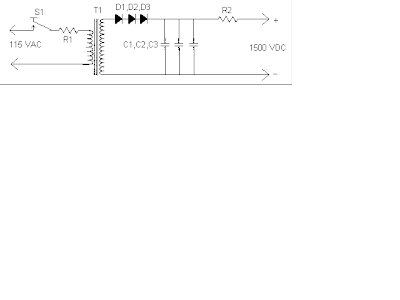
Notes
1. T1 is an ordinary 9V 1A transformer connected backwards for step up.
2. R1 MUST be installed on a LARGE heatsink. A good heatsink is the metal case the supply is built in.
3. R2 Protects the laser tube from excess current. It should be soldered directly to the anode terminal on the tube. To find R2, start with a 500K 10W resistor and work down until the tube lights and remains stable.
4. If you have trouble with the tube not starting easily, use a longer anode lead that is wrapped around the tube.
5. Depending on the transformer you use, the schema may or may not work. I cannot guarantee the operation of this schema. Build at your own risk. Some transformers contain very few secondary windings which will quickly saturate the core and basically act like a direct short. The more secondary windings (that is, primary in this schema) the better.
Via
Subscribe to:
Posts (Atom)
