Showing posts with label using. Show all posts
Showing posts with label using. Show all posts
Thursday, November 13, 2014
Automatic car parking indicator using Microcontroller Description Conventionally car parking systems does not have any intelligent monitoring syste

Conventionally, car parking systems does not have any intelligent monitoring system. Parking lots are monitored by human beings. All vehicles enter into the parking and waste time for searching for parking slot. Sometimes it creates blockage. Condition become worse when there are multiple parking lanes and each lane have multiple parking slots.
Use of automated system for car parking monitoring will reduce the human efforts. Display unit is installed on entrance of parking lot which will show LEDs for all Parking slot and for all parking lanes. Empty slot will be indicated by glowing the respective LED.
We have used Infra Red transmitters and Receivers for each parking slot. The IR Receivers are connected to AVR microcontroller. IR rays are obstructed when a car is parked in any parking slot. Thus AVR will come to know that which slot is empty and which slot is full. We have chosen IR module instead of RF module because we want a receiver having line of sight communication with the transmitter. But RF does not require line of sight communication. And in case of LDR, there is scope for false triggering due to sunlight or headlight of car. So considering all these points we have finalized to use IR module. For transmitter section we are going to use IR LEDs driven by a 555 timer IC. Timer IC will generate a frequency of 38 KHz, which will be given to IR LED

LED Sound level display circuit by using IC LM3915
This circuit is about audio sound level LED display, indicator, monitor or you can say it “Audio VU (Volume Unite) Meter”.
This is a simple audio sound level LED display circuit diagram. The circuit is completely based on a single ic LM3915 from National Semiconductor. The LM3915 is a monolithic integrated circuit. It displays the audio sound level in terms of 10 LEDs and providing a logarithmic 3 dB/step analog display.
This is a simple audio sound level LED display circuit diagram. The circuit is completely based on a single ic LM3915 from National Semiconductor. The LM3915 is a monolithic integrated circuit. It displays the audio sound level in terms of 10 LEDs and providing a logarithmic 3 dB/step analog display.
Audio sound level display circuit diagram
 |
| Fig: Circuit diagram of sound level display using ic LM3915 |
The audio sound level LED display circuit can operate from a single supply 3V to 25V. But I suggest to use 9-12V. LED brightness can be controlled with a single pot( variable resistor) as shown 10K ohm in the circuit. Connect the audio input signal in Pin-5 of LM3915 from output of a audio device like output of audio amplifier or any other source.
The Pin-9 of LM3915 is to select dot or bar mode display. To make the circuit moving dot display instead of a bar graph display disconnect the Pin-9 from +V. Friday, November 7, 2014
50 W Power Amplifier Circuit using STK084

This is the circuit diagram of 50W power amplifier circuit which built based on single power amplifier chip of STK084. Its an well-known old IC for audio frequency (AF) amplifier.
This circuit requires dual polarity / split power supply with maximum supply of ± 50. The recommended supply is ± 35 / 2-3A DC current. You may use this split power supply circuit for the amplifier. Use 28V center tap transformer to get about ± 36V output.
Technical Details:
Power output: 50W
RL : 8 Ohm
TDH : 0.2 %
Rin : 52K
Gain : 26.4 dB
Noise : 0.3 mV
RL : 8 Ohm
TDH : 0.2 %
Rin : 52K
Gain : 26.4 dB
Noise : 0.3 mV
Take a note that heatsink is required to be mounted on the power IC since it will going to hot when operated and deliver high power output (high audio volume level).
Tuesday, November 4, 2014
Metal Detector Circuit Schematic using Beat Frequency Oscillator BFO
The simplest method of detecting metal is by beat frequency oscillator. The circuit basically consists of two balanced oscillator. One acts as the detector element, the other provides the reference signal. This oscillator frequency reference is set to fix value, whilst the detector oscillator varies depending on the metal presence. The reference oscillator can be constructed using various circuit topology: inductor-capacitor (LC), resistor-capacitor (RC), or even a crystal (quartz) oscillator. While the reference oscillator can be implemented using various circuit topology, the detector oscillator always use inductor-capacitor topology, because the mechanism will be using the magnetic induction property of the detected object, and the inductor component of the detector oscillator will be the detecting probe.
With the absence of a metal near the detector probe (the inductor component of the detector oscillator), the detector oscillator is tuned to have same frequency as the reference oscillator. The output of the detector oscillator and the reference oscillator output is mixed using hetero-dyne mixer circuit, producing a beat frequency output of zero Hz, or a very low frequency if both oscillator is slightly unbalanced. In the presence of a metal near the detector probe, the detector oscillator will shift it’s frequency, and the mixer output will produce a tone with frequency equal to the difference of the reference and the detector frequency.
The figure below shows one of the simple metal detector circuit.You can see the reference circuit is a simple RC circuit, and its frequency is determined by R1-P2-C1. The detector oscillator is an LC oscillator with the frequency is determined by the L1-C2-C3 values.
The NAND gates use CMOS 4011 chip, a low power component that is suitable for this battery-operated circuit. You can see that this chip is supplied by a 5V voltage coming from an LM7805L regulator. You might wonder what the purpose of this regulation is, since the power supply come from a 9V battery and the CMOS gates can handle the voltage of 3-15 Volt. The main purpose of the regulator is to keep a constant voltage source for the reference oscillator frequency stability, since the frequency is affected by the power supply voltage variation as the battery voltage drops in the long time of usage.
Here the complete parts list:
Parts list:
U1: CD4011
U2: LM389
U3: 78L05
R1: 2.2k 5%
P2: 4.7k lin.
R3: 330k 5%
R4: 270k 5%
R5: 1k 5%
C1: 390pF (NPO)
C2,C3,C4: 10nF
C5: 10uF 16v electrolytic
C6,C8: 220 uF 16v electrolytic
C7: 100uf 16v electrolytic
C9: 100nF ceramic
P1: 4.7k log
L1: 22cm in diameter with 14 turns AWG 26
K1: SPDT toggle switch
J1= Headphone jack 1/4 or 1/8 inch
Other parts: 9v battery connector, speaker or headphones
To tune the circuit, plug a headphone at the output, and remove any metal around the inductor L1. Set the volume control P1 around at center. Set the reference oscillator tuner P2 at the maximum or minimum position, you should hear no sound since the frequency should be in ultrasonic range. Turn slowly P2 until you hear a very high audio frequency, continue turning the pot until the frequency is decreasing and stop turning when the note is just disappeared (the frequency is decreased down below 20 Hz). After this, you can test the circuit by placing a metal near the inductor L1 and now the output will give an audible frequency as the detection alert.
Read More..
With the absence of a metal near the detector probe (the inductor component of the detector oscillator), the detector oscillator is tuned to have same frequency as the reference oscillator. The output of the detector oscillator and the reference oscillator output is mixed using hetero-dyne mixer circuit, producing a beat frequency output of zero Hz, or a very low frequency if both oscillator is slightly unbalanced. In the presence of a metal near the detector probe, the detector oscillator will shift it’s frequency, and the mixer output will produce a tone with frequency equal to the difference of the reference and the detector frequency.
The figure below shows one of the simple metal detector circuit.You can see the reference circuit is a simple RC circuit, and its frequency is determined by R1-P2-C1. The detector oscillator is an LC oscillator with the frequency is determined by the L1-C2-C3 values.
The NAND gates use CMOS 4011 chip, a low power component that is suitable for this battery-operated circuit. You can see that this chip is supplied by a 5V voltage coming from an LM7805L regulator. You might wonder what the purpose of this regulation is, since the power supply come from a 9V battery and the CMOS gates can handle the voltage of 3-15 Volt. The main purpose of the regulator is to keep a constant voltage source for the reference oscillator frequency stability, since the frequency is affected by the power supply voltage variation as the battery voltage drops in the long time of usage.
Here the complete parts list:
Parts list:
U1: CD4011
U2: LM389
U3: 78L05
R1: 2.2k 5%
P2: 4.7k lin.
R3: 330k 5%
R4: 270k 5%
R5: 1k 5%
C1: 390pF (NPO)
C2,C3,C4: 10nF
C5: 10uF 16v electrolytic
C6,C8: 220 uF 16v electrolytic
C7: 100uf 16v electrolytic
C9: 100nF ceramic
P1: 4.7k log
L1: 22cm in diameter with 14 turns AWG 26
K1: SPDT toggle switch
J1= Headphone jack 1/4 or 1/8 inch
Other parts: 9v battery connector, speaker or headphones
To tune the circuit, plug a headphone at the output, and remove any metal around the inductor L1. Set the volume control P1 around at center. Set the reference oscillator tuner P2 at the maximum or minimum position, you should hear no sound since the frequency should be in ultrasonic range. Turn slowly P2 until you hear a very high audio frequency, continue turning the pot until the frequency is decreasing and stop turning when the note is just disappeared (the frequency is decreased down below 20 Hz). After this, you can test the circuit by placing a metal near the inductor L1 and now the output will give an audible frequency as the detection alert.
Friday, October 31, 2014
300 Watt MOSFET Broadband Amplifier Using MRF141G

The following segment will provide the enhanced Motorola schematic for any typical application for the MRF141G (which includes parasitic stabilization features), a broadband power RF MOSFET which will place out a conservatively-rated 300 watts across the FM broadcast band. The flange about the MRF141G ought to be mounted to a heat spreader, a copper plate 5/16" thick and 6" x 8", which is then mounted to the heatsink with 6-32 machine screws, if your heatsink is drilled and tapped.
I recommend getting the two transformer assemblies, instead of trying to create them, due to the fact 15-ohm hardline is not straightforward to come across.
Thursday, October 30, 2014
Mini Stereo Power Amplifier using TDA2822
This circuit TDA2822 total to the same extent your primary device. The Dual Amplifier IC before IC stereo increase by 40 dB. Bandwidth 120 kHZ. with the purpose of is regarding 2 watts and watt power supply of 1.8 to 15 volts and a current 6 mA no more than after using the power supply 9 volt into this circuit.VR1 and VR2 to adjust the suggest level of the best and not here, the pin 7 and pin 6 of IC1.The amplifier IC1 is outmoded of the output pin 1 and pin 3, through the C4 and C5 coupling signals to the absent and right speakers.The C6, R1 and C7, R2 is to reduce blast.
 |
| Mini Stereo Power Amplifier using TDA2822 Circuit Diagram |
On Demand WC Fan Using 555 Circuit Diagram
In most WCs with an extractor the fan is connected to the lighting circuit and is switched on and off either in sympathy with the light or with a short delay. Since toilets are sometimes used for washing the hands or just for a quick look in the mirror, it is not always necessary to change the air in the smallest room in the house. The following circuit automatically determines whether there really is any need to run the fan and reacts appropriately. No odour sensor is needed: we just employ a small contact that detects when and for how long the toilet seat lid is lifted.
On-Demand WC Fan circuit Using 555
If the seat lid is left up for at least some presettable minimum time t1, the fan is set running for another presettable time t2. In the example shown the contact is made using a small magnet on the lid and a reed switch mounted on the cistern. The rest is straightforward: IC2, the familiar 555, forms a timer whose period can be adjusted up to approximately 10 to 12 minutes using P2. This determines the fan running time. There are three CMOS NAND gates (type 4093) between the reed switch and the timer input which generate the required trigger signal. When the lid is in the ‘up’ position the reed switch is closed.
Capacitor C1 charges through P1 until it reaches the point where the output of IC1a switches from logic 1 to logic 0. The output of IC1b then goes to logic 1. The edge of the 0-1 transition, passed through the RC network formed by C2 and R2, results in the output of IC1c going to logic 0 for a second. This is taken to the trigger input on pin 2 of timer IC2, which in turn switches on the relay which causes the fan to run for the period of time determined by P2. The circuit is powered from a small transformer with a secondary winding delivering between approximately 8 V and 10 V. Do not forget to include a suitable fuse on the primary side.
The circuit around IC1b and IC1c ensures that the fan does not run continuously if the toilet seat lid is left up for an extended period. The time constant of P1 and C1 is set so that the fan does not run as a result of lavatorial transactions of a more minor nature, where the lid is opened and then closed shortly afterwards, before C1 has a chance to charge sufficiently to trigger the circuit.
Sunday, October 5, 2014
2N3055 using ic 5 Volt Linear power supply regulator

This is 5 Volt Linear power supply regulator circuit. It uses electronics part that seek easily have no zener diode , and the integrated circuit use Transistor 2N3055 and other. Which seek easily use diode perform heal voltage be stable. By diode 1N914 number uses 1N4148 number can replace. For Transistor 2N3417 use the number BD139 equiv get. If use Transformer 1-2A circuit be this size give current get about 1 Amp. Friends may don’t be bored with line this circuit. I thinks it may advantage seek part easy and economize good yes.
Thursday, October 2, 2014
Low Battery Monitor Circuit Using SCR
The prototype of this device will be used in a hospital operating theatre in unijnction with battery operated medical equipment (powered by four pen-light cells).
A moving coil voltmeter was not appropriate as, in the designers’ experience, medical staff have difficulty in interpreting a voltmeter and sometimes find themselves half way through an` operation with exhausted batteries. Therefore, the requirements for the indicator were that: 1) the display be eye catching, easily understandable and provide a sense of urgency as · the battery approaches exhaustion; 2) provide adequate warning of battery failure (at least ‘l hour); 3) current consumption of the indicator be low in. relation to the main equipment; 4) preferably, be more rugged and cheaper than a moving coil meter. The design was based on a programmable unijunction transistor (PUT), because its threshold characteristics can be well defined, arranged to flash a light emitting diode (L.E.D.) indicator. The circuit is shown in the figure. The PUT (Q1) is used in a relaxation oscillator circuit. As the voltage being monitored (Vm,,,,) falls, the voltage on the gate (Vg) falls whilst the anode voltage (V,) remains essentially constant. Oscillation commences when V, falls below V, by 0.6 volts. As Vm, falls further, Vg falls and the PUT triggers at lower values of Va. Thus the cycle time shortens and the frequency of flashing increases giving a sense of urgency as the battery approached exhaustion. Transistor O2 and C2 act as a pulse stretcher and amplifier to drive the L.E.D. display. In the prototype the trigger point can be adjusted from 4.5-5.5 volts and the current drain when V,,,,,,, is 6 volts is 1 mA (controlled primarily by R1). This is considered acceptable as the device being monitored draws 17 mA. All the requirements have been met. The components of this low battery monitor circuit are mounted on the printed circuit board of the main device.
A moving coil voltmeter was not appropriate as, in the designers’ experience, medical staff have difficulty in interpreting a voltmeter and sometimes find themselves half way through an` operation with exhausted batteries. Therefore, the requirements for the indicator were that: 1) the display be eye catching, easily understandable and provide a sense of urgency as · the battery approaches exhaustion; 2) provide adequate warning of battery failure (at least ‘l hour); 3) current consumption of the indicator be low in. relation to the main equipment; 4) preferably, be more rugged and cheaper than a moving coil meter. The design was based on a programmable unijunction transistor (PUT), because its threshold characteristics can be well defined, arranged to flash a light emitting diode (L.E.D.) indicator.
Thursday, September 18, 2014
7 Watt Audio Amplifier Using TDA2003
Schematic diagram of a simple 7 watt audio amplifier using TDA2003 Amplifier IC. This is a good IC with many built in features like low harmonic distortion, short schema protection,thermal overload protection etc. This IC is a upgrade version of TDA 2002 amplifier IC.
7 Watt Audio Amplifier Circuit Diagram :

The schema is small and using only few components and it is able to deliver 7w output on 12V DC. Assamble the schema on PCB or veroboard and use heatsink with IC. Input voltage can be between 8 to 18 volt / 0.5A DC.
Friday, September 5, 2014
Touch Switch Using FET
The series of touch this switch be an Touch Switch made using FET. This circuit serves to activate electronic devices only when we touch touch sensors.
Once we release a touch to the sensor, the electronic device that is connected is turned off again. The series of touch switch or touch switch is very simple, composed only of a FET, resistor and capacitor. The series of touch switches / touch switches work with source voltage 12VDC. Detailed series of touch switches / touch switch can be seen in thethe following figure .
Once we release a touch to the sensor, the electronic device that is connected is turned off again. The series of touch switch or touch switch is very simple, composed only of a FET, resistor and capacitor. The series of touch switches / touch switches work with source voltage 12VDC. Detailed series of touch switches / touch switch can be seen in thethe following figure .
FET Touch Switch
The series of touch switches / touch switch can only be used to illuminate DC, 12V DC lamp when it replaced the relay, the circuit can be used safely to load the AC network. Sensor touch to this series was made with 2 pieces of plate are arranged close together (within 1-2mm).
Monday, September 1, 2014
Switching Mode Power Supply using STR
| Switching power supply |
This power supply circuit is a type SMPS (Switching Mode Power Supply) using mosfet transistor integrated circuit voltage controller in one IC package, namely STR-W6654. This IC will control the duty cycle of time off Vth2 Mosfet transistor to control the output voltage. Besides, the IC is also equipped with a safety circuit against overvoltage (OVP), overcurrent (OCP) and over temperature (TSD) circuit is working on 220V ac voltage with the input ac voltage range of 176V to 260V ac or known by the Wide range Regulators.
How to Work Series
Initial bias voltage dc pin6 IC801 obtained from an ac voltage through D811 and R817, in the beginning of this pin6 high input impedance, or simply need a current of about 100uA, if the voltage has reached the 10V, the IC will mendrive Mosfet transistor into On and transformer will generate stress induction through V1 , R819 and D816 making this pin6 voltage rises to 16V working voltage, and at this point impedance pin6 will shrink or current will increase to 30mA.
Voltage Stabilizer
Stabilizing the output voltage of the circuit is done by regulating the length of time off of the transistor current MOSFETs by using the feedback coupler photo released by the D807. And the D807 is controlled by the IC regulator IC802, IC is working based on the transformer secondary winding S2 (main output). Change IC802 PIN1 perceived stress will be informed on the photo coupler D807 and forwarded to the IC801 for correction.
Safety Over Voltage
In the event of errors / defects in the feedback path, the output voltage will rise out of control, but the series / IC801 has been equipped with a safety overvoltage, where pin6 IC801 can serve as a detection voltage, output voltage rises when the voltage V1 uncontrolled transformer also rises and via the R819, D816 IC801 pin voltage also rose, When the voltage reaches 34V in IC801 oscillator will stop / off switch and voltage pin6 will go down, and when the voltage reaches 7.5 V IC is going back to work and pin6 voltage rises again, if it again reaches 34V IC will die, so planes demikiian will be dead-alive, dead-alive.
Safety Flow / Cost More
The series is able to secure the power supply circuit to the flow or more load by detecting current flowing in the drain-source transistors MOSFETs. By placing a resistor R809, R835, and R811 on pin3 (source) and connected to pin7 (OCP), the more current or voltage drop on this resistor can be directly detected by a safety circuit overcurrent (OCP). In the event of overload or over current IC will stop for pin 6 voltage above 7.5V
Safety Over Temperature
IC STR-W6654 is also equipped with over temperature safety circuit (TSD). If an error occurs in the IC cooling load or metal, can cause uncontrolled temperature rise IC if IC exceeds 140 degrees then it will stop. The aircraft can live again when the voltage is below 7.5V pin6 (main switch is turned off) and the temperature has dropped below 140 degrees.
Stand-By Condition
With working characteristics pin6 tapped IC STR-W6654 especially voltage Latch Circuit Release Voltage (7.5V) the IC can be made to work on a very small load conditions (stand-by)
How it works series Stand-By
In normal conditions PIN1 UOC IC output is 5V (high) and on stand-by condition 0V (low). If the output of PIN1 UOC Low, Q852 off, Q857 is on, thus the input voltage to 10V PIN2 of IC 802 that will cause the output voltage to 52 volts IC801 PIN1. Thats due to the influence of input voltage PIN1 decreased from 26 V to 10V. so that the circuit feed back will inform you as there is more current. IC 801 IC801 stop temporarily until voltage falls below 7.5V pin6. After reaching 7.5V IC801 automatically revived. So this event will be repeated with certain intervals. The fall in line with all automatic 90V secondary circuit also fell, including PIN1 (V1) transformer. If the transformer voltage drop V1 also fell tentunnya pin6 IC801, IC801 will follow the working characteristics pin6.
In the event of errors / defects in the feedback path, the output voltage will rise out of control, but the series / IC801 has been equipped with a safety overvoltage, where pin6 IC801 can serve as a detection voltage, output voltage rises when the voltage V1 uncontrolled transformer also rises and via the R819, D816 IC801 pin voltage also rose, When the voltage reaches 34V in IC801 oscillator will stop / off switch and voltage pin6 will go down, and when the voltage reaches 7.5 V IC is going back to work and pin6 voltage rises again, if it again reaches 34V IC will die, so planes demikiian will be dead-alive, dead-alive.
Safety Flow / Cost More
The series is able to secure the power supply circuit to the flow or more load by detecting current flowing in the drain-source transistors MOSFETs. By placing a resistor R809, R835, and R811 on pin3 (source) and connected to pin7 (OCP), the more current or voltage drop on this resistor can be directly detected by a safety circuit overcurrent (OCP). In the event of overload or over current IC will stop for pin 6 voltage above 7.5V
Safety Over Temperature
IC STR-W6654 is also equipped with over temperature safety circuit (TSD). If an error occurs in the IC cooling load or metal, can cause uncontrolled temperature rise IC if IC exceeds 140 degrees then it will stop. The aircraft can live again when the voltage is below 7.5V pin6 (main switch is turned off) and the temperature has dropped below 140 degrees.
Stand-By Condition
With working characteristics pin6 tapped IC STR-W6654 especially voltage Latch Circuit Release Voltage (7.5V) the IC can be made to work on a very small load conditions (stand-by)
How it works series Stand-By
In normal conditions PIN1 UOC IC output is 5V (high) and on stand-by condition 0V (low). If the output of PIN1 UOC Low, Q852 off, Q857 is on, thus the input voltage to 10V PIN2 of IC 802 that will cause the output voltage to 52 volts IC801 PIN1. Thats due to the influence of input voltage PIN1 decreased from 26 V to 10V. so that the circuit feed back will inform you as there is more current. IC 801 IC801 stop temporarily until voltage falls below 7.5V pin6. After reaching 7.5V IC801 automatically revived. So this event will be repeated with certain intervals. The fall in line with all automatic 90V secondary circuit also fell, including PIN1 (V1) transformer. If the transformer voltage drop V1 also fell tentunnya pin6 IC801, IC801 will follow the working characteristics pin6.
Sunday, August 31, 2014
Simple Programmable Bandpass using twin t bridge
The Simple Programmable Bandpass using twin-t bridge schema gives a programmable bandpass where both the cut-over frequency and the gain, A, are controlled independently. In the twin-T bridge the resistors R and R/2 are replaced by two double FETs, 430, the channel resistance of the first one in the series, the channel resistances of the second one are in parallel as to stimulate the resistance R/2. Both these resistors are controlled by Vc which ranges from 0 V to about 1 V. The gain of the schema is set by means of the resistors R2 and R3.
Simple Programmable Bandpass using twin-t bridge Circuit Diagram
Saturday, August 30, 2014
Long range Burglar Alarm Using Laser Torch
Laser torch-based burglar alarms normally work in darkness only. But this long-range photoelectric alarm can work reliably in daytime also to warn you against intruders in your big compounds, etc. The alarm comprises laser transmitter and receiver units, which are to be mounted on the opposite pillars of the entry gate. Whenever anyone enters to interrupt the transmitted laser beam falling on the receiver, the buzzer in the receiver schema sounds an alarm.
The range of this burglar alarm is around 30 metres, which means you can place the transmitter and the receiver up to 30 metres apart. Since the laser torch can transmit light up to a distance of 500 metres, this range can be increased by orienting the phototransistor sensor properly. To avoid false triggering by sunlight, mount the phototransistor sensor such that it doesn’t directly face sunlight.
Long-range Burglar Alarm Using Laser Torch
The transmitter schema is powered by 3V DC. The astable multivibrator built around timer 7555 (IC1) produces 5.25kHz frequency. CMOS version of timer 7555 is used for low-voltage operation. The body of the laser torch is connected to the emitter of npn transistor T1 and the spring-loaded lead protruding from inside the torch is connected to the ground.
The receiver schema is powered by 12V DC. It uses photoDarlington 2N5777 (T2) to sense the laser beam transmitted from the laser torch. The output beam signals from photoDarlington are given to the two-stage amplifier followed by switching schema, etc. As long as the laser beam falls on photoDarlington T2, relay RL1 remains un-energised and the buzzer does not sound. Also, LED1 doesn’t glow.
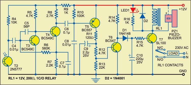
Fig. 2: Receiver schema
When anyone interrupts the laser beam falling on photoDarlington T2, npn transistor T6 stops conducting and npn transistor T7 is driven into conduction. As a result, LED1 glows and relay RL1 energises to sound the buzzer for a few seconds (determined by the values of resistor R15 and capacitor C10). At the same time, the large indication load (230V AC alarm for louder sounds or any other device for momentary indication) also gets activated as it is connected to 230V AC mains via normally opened (N/O) contact of relay RL1.
Sourced By: EFY Author ; Pradeep G.
Alarm using your own Voice
This alarm plays your prerecorded voice message. It is built around the readily available quartz clock. Take the buzzer out of the quartz clock and connect its positive terminal to pin 1 and negative terminal to pin 2 of optocoupler IC MCT2E (IC2). Pin 4 of IC2 is grounded and pin 5 is connected to trigger pin 2 of monostable multivibrator IC 555 (IC3) as shown in Fig. 2.
Fig. 1: Voice recording schema
Fig. 1 shows the schema for recording your voice message. When you press switch S2, it plays the meassage. The control schema shown in Fig. 2 avoids the need for pressing switch S2 and thereby sounding the voice alarm automatically at the preset time.
Connect points A and B of the recording schema to the corresponding points A and B of the control schema. After making the connections, press record switch S1 to record your 6-second voice message through condenser microphone. Set the desired alarm time in quartz clock. At the time of alarm, buzzer terminals provide voltage to the internal LED of optocoupler IC2. This results in conduction of internal transistor of IC2, and its collector voltage at pin 5 drops to trigger IC3. The output of IC3 goes high for approximately 6 seconds. During this period, the prerecorded message is heard continuously. The message repeats every 6 seconds. The sound is loud enough in a room.
Fig. 2: Voice control schema
The schema operates off 3 volts and it can be easily fitted in a small box and fixed on the back side of the alarm quartz clock.
Sourced by: EFY Author: Naga Babu Araya
Saturday, August 23, 2014
Simple Car alarm Wiring diagram Schematic Using 555 Timer
This is a Simple Car alarm Circuit Diagram Using 555 Timer.In this simple schema 555 timer produces a guaranteed delay, allowing the driver to deactivate the alarm and the elimination of a control switch vulnerable outside.The RCS prevents triggering a timer timer B, unless B is triggered by timer switches strategically located detector.
Simple Car alarm Circuit Diagram Using 555 Timer
Wednesday, August 20, 2014
PWM Controller Circuit using SN75603 and SN75604

Here the schema diagram of PWM Controller which uses complementary half-H peripheral drivers SN75603 and SN75604, with totem-pole outputs rated at 40 V and 2.0 A. These drivers effectively place the motor in a full-bridge configuration, which has the ability to provide bidirectional control.
Timer U1 operates in the astable mode at a frequency of 80 Hz. The 100-Ω discharge resistor results in an 8-μs trigger pulse which is coupled to the trigger input of timer U2. Timer U2 serves as the PWM generator. Capacitor C1 is charged linearly with a constant current of 1 mA from the 1N5297, which is an FET current-regulator diode. Motor speed is controlled by feeding a dc voltage of 0 to 10 V to control input pin 5 of U2. As the control voltage increases, the width of the output pulse pin 3 also increases. These pulses control the on/off time of the two motor drivers. The trigger pulse width of timer U1 limits the minimum possible duty cycle from U2.
Tuesday, August 19, 2014
Adjustable Symmetrical Power Supply Using LM317 and LM337
The schema was designed to provide an adjustment with a power supply that is symmetrically designed while providing a voltage range of 1.25V to 30V at 1A current. LM317 – an adjustable 3-terminal positive voltage regulator capable of supplying in excess of 1.5A over an output voltage range of 1.2V to 37V and requires only two external resistors to set the output voltage due to its internal current limiting, thermal shutdown and safe area compensation, making it essentially blow-out proof LM337 – an adjustable 3-terminal positive voltage regulator capable of supplying in excess of 5A used as battery chargers, constant current regulators, and adjustable power supplies due to its features such as protected output from short schema, product enhancement tested, current limit constant with temperature, guaranteed thermal regulation, adjustable output down to 1.2V, guaranteed 5A, and guaranteed 7A peak output current.
The schema will serve as a voltage converter with an input voltage of 35 V to produce an output voltage of 1.25 V to 30 V. The positive voltage is being handled by LM317 IC while the negative voltage is handled by LM337. The schema can provide an output current of 1 A. During the production of 1 A current, the regulator is dissipating too much heat and without the presence of a heatsink, the regulator may get damaged.
Using these types of regulators provide features such as low noise and low price in the market. It can be made operational even with few components used. The only disadvantage that it will impose is the poor conversion efficiency. With the output of 35 V to 5 V, the efficient ratio of the output power with the input power is less than 42%. This is the reason why the switching regulator became cheap recently although the number of external components to be connected is minimally increased. These regulators will work with better efficiency when used in case where current is more than 1A for more than 15 V and 0.4 A for less than 15 V from the power supply. Each regulator is adjusted for single positive and negative voltage output using the 10K ohms potentiometers RV1 & RV2. For dual outputs, a dual connected potentiometer RV3 is made to operate by switch S1. The visual indication on the voltmeter V1 is shown using the switch S2.
Using these types of regulators provide features such as low noise and low price in the market. It can be made operational even with few components used. The only disadvantage that it will impose is the poor conversion efficiency. With the output of 35 V to 5 V, the efficient ratio of the output power with the input power is less than 42%. This is the reason why the switching regulator became cheap recently although the number of external components to be connected is minimally increased. These regulators will work with better efficiency when used in case where current is more than 1A for more than 15 V and 0.4 A for less than 15 V from the power supply. Each regulator is adjusted for single positive and negative voltage output using the 10K ohms potentiometers RV1 & RV2. For dual outputs, a dual connected potentiometer RV3 is made to operate by switch S1. The visual indication on the voltmeter V1 is shown using the switch S2.
- R1-2=270ohms
- R3-4=2.2Kohms
- R5-6=10Kohms
- C1-5=100uF/63V
- C2-4=100nF/100V
- C3-8=10uF/25V
- C6-10=100uF/63V
- C7-9=100nF/100V
- RV1-2=10Kohms Lin.
- RV3=2X10Kohms Lin.
- IC 1=LM 317T
- IC 2=LM 337T
- D1-2=1N4001
- D3-4=1N4001
- L1-2=LED 3mm
- F1-2=1A slow Blow Fuse
- S1-2=2X ON-ON SW
- V1=0-30V DC Voltmeter
The adjustable symmetrical power supply is suitable to be used in audio amplifiers, microphone amplifiers, op-amp applications, impedance converters and other devices that require regulated positive and negative DC supply, since the output current is 1 A.
Monday, August 18, 2014
Variable Power Supply Using LM723
Using LM723 regulator can be designed a very simple variable power supply schema which can provide a maximum current up to 2A and a variable voltage between 2 and 25 volts.This 25v variable power supply is designed using a LM723 regulator and a few common electronic components.Input voltage must be between 28 and 37 volts. Mj3000 transistor must be mounted on a radiator for heat dissipation.
LM723 Variable Power Supply Circuit diagram

LM723 Variable Power Supply Circuit diagram

Friday, August 15, 2014
Using LED as a diode Rectifier Wiring diagram Schematic
This is a simple LED as a diode Rectifier Circuit Diagram. In certain situations where the current is not high, we can use the famous LED (LED) and diode rectifier voltage power diagram. The LED can be used without problem in a rectification schema, and also works in the power ratings. Pay attention not to exceed the maximum current of the LED in a wave rectifier.
Using LED as a diode Rectifier Circuit Diagram

Subscribe to:
Posts (Atom)
