A circuit for monitoring supply voltages of ±5 V and ±12 V is readily constructed as shown in the diagram. It is appreciably simpler than the usual monitors that use comparators, and AND gates. The circuit is not intended to indicate the level of the inputs. In normal operation, transistors T1 and T3 must be seen as current sources. The drop across resistors R1 and R2 is 6.3 V (12 –5 –0.7). This means that the current is 6.3mA and this flows through diode D1 when all four voltages are present. However, if for instance, the –5 V line fails, transistor T3 remains on but the base-emitter junction of T2 is no longer biased, so that this transistor is cut off. When this happens, there is no current through D which then goes out.
Showing posts with label supply. Show all posts
Showing posts with label supply. Show all posts
Wednesday, November 19, 2014
Odd Block KT88 Series 1 Tube Amp Power Supply
A schematic of the ability accumulation is apparent below. Like the amplifier schematic, the ability accumulation ambit is © OddWatt Audio and permission to host the schematic on this armpit has been provided by OddWatt Audio. You are chargeless to use the schematic for personal, non-commercial use.
Mains ability enters the amplifier through an IEC atrium amid at the rear of the amp. The IEC atrium includes a 3 Ampere agglutinate and an EMI filter. The ability agent is an OEM bogus by Edcor with ratings of 180V-0-180V at 250 mA and 12V at 4A. Ability accumulation capacitors are Panasonic ECG alternation 500 volt electrolytic and Solen Polypropyene. The ample ability resistors are Vishay/Dale wire anguish and the actual resistors are carbon film. The High-Tension (HT) accumulation is rectified with STTH5 ultrafast aerial voltage rectifiers and uses CRC filtering. A 12V DC accumulation is acclimated for the tube heaters. An adjustable adjournment ambit is acclimated to adjournment the HT accumulation on ability up.
Tuesday, November 18, 2014
10A High Current variable power supply
Power supply has 10A maximum current and output voltage can be set from 2 - 36VDC. Power supply circuit is quite simple, which is composed of the rectifier, voltage regulator and power regulator. Power regulator circuit High Current Variable Power Supply 10A uses the Q3 and Q4 are arranged Darlington and serves as a power regulator drivers Q5 and Q6. While the voltage regulator circuit is VR1 which serves as a variable voltage divider and Q1 and Q2 are arranged as a controller driver Darlington power regulator with variable reference voltage divider VR1.
In a series of High Current Variable Power Supply 10A 10A above have been completed as a current-limiting fuse. and to monitor the current flowing with ampere meter and volt meter to monitor the output voltage of the circuit.
Monday, November 17, 2014
5 Volt Switching Regulator Power Supply
The switching regulator power supply used LM2575-5.0 on this schematic. You can make the stable voltage by using the 3 terminal regulator like LM317. However, because the output electric current and the inputted electric current are the same approximately, the difference between the input electric power (The input voltage x The input electric current) and the output power (The output voltage x The output current) is consumed as the heat with the regulator. Because it is, the efficiency isn't good. 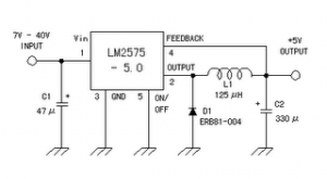
Data sheet for LM2575
SIMPLE SWITCHER 1A Step-Down Voltage Regulator
http://www.national.com/pf/LM/LM2575.htm
Read More..
Data sheet for LM2575
SIMPLE SWITCHER 1A Step-Down Voltage Regulator
http://www.national.com/pf/LM/LM2575.htm
Friday, November 14, 2014
5V DC POWER SUPPLY


Thursday, November 6, 2014
Saturday, October 25, 2014
IC TLC271 Single supply Function Generator
The circuit has both square-wave and triangle-wave output. The left section is similar in function to a comparator circuit that uses positive feedback for hysteresis. The inverting input is biased at one-half the Vcc voltage by resistor R4 and R5. The output is fed back to the non-inverting input of the first stage to control the frequency.
The amplitude of the square wave is the output swing of the first stage, which is 8V peak-to-peak. The second stage is basically an op amp integrator.
Saturday, October 18, 2014
2N3055 UA723 Power Supply Adjustable 0 30V 2A

It is a simple circuit regulated power supply, based on the known UA723, that drive a transistor Q1 [2N3055]. The regulation of voltage, of expense becomes with potentiometer R1 from 0v-30v DC roughly. In order to we achieve 30 V, will should the transformer of supply TR1, it gives all the current that it asks the load, differently the output voltage it will be found in the levels of 26 V roughly. Essential is the use of a good heatsink for transistor Q1, as well as good quality of potentiometer in the place of R1.
Source:http://users.otenet.gr/~athsam/power_supply_30.htm
Sunday, October 5, 2014
2N3055 using ic 5 Volt Linear power supply regulator

This is 5 Volt Linear power supply regulator circuit. It uses electronics part that seek easily have no zener diode , and the integrated circuit use Transistor 2N3055 and other. Which seek easily use diode perform heal voltage be stable. By diode 1N914 number uses 1N4148 number can replace. For Transistor 2N3417 use the number BD139 equiv get. If use Transformer 1-2A circuit be this size give current get about 1 Amp. Friends may don’t be bored with line this circuit. I thinks it may advantage seek part easy and economize good yes.
36V Output L200 Power Supply Circuit

Description
Power supply with variable voltage and fixed current regulation made using the ubiquitous L200C regulator.
Notes
The versatile 5 pin L200C regulator offers both voltage and current regulation in a single package. The IC also features thermal shutdown and input over voltage protection up to 60 Vdc. The package is also available as L200CV which has straight pins for mounting onto a PCB. The above circuit has current limiting of 1 amp, hence Rsc = 0.45 ohm. The output voltage is variable from 2.85V to 36V. For voltages up to 36V then the input voltage, Vcc must be 40V. The supply voltage must always a few volts higher than the maximum output voltage. If you wanted to make a 9 Volt current limited PSU then the input voltage should be a minimum of 12 Volts.
Maximum Power Dissipation
The L200 has internal limiting to reduce the amount of heat dissipation. This happens when the internal junction temperature reaches 150 °C. The datasheet has a graph of the safe operating area, but if drawing maximum output current of 2 amp, the input voltage minus output voltage difference must be less than 20 Volts.
Specifications:
DC Input Voltage: 40V max.
Peak Input Voltage: 60V max. for 10ms
Output Voltage Range: 2.85 to 36V
Output Current Range: 0.1 to 2A
Quiescent Current: 4.2mA
Output Noise: 80uV
The L200 regulator has many versions; L200, L200C, L200CH, L200CV. These are in fact all the same regulator. The main differences between variations are the thermal junction temperature and pinout.
For the L200, the operating junction temperature is -55 to 150 °C
The L200C operating junction temperature is -25 to 150 °C.
The V stands for vertical and is the most common case style; available as a pentawatt package, shown right hand side. The H stands for horizontal and the pins of the L200 are bent at right angles for PCB mounting. The L200T and L200CT are also available but as a TO3-4 layout, this pinout can be seen in the datasheet, link below
Friday, September 19, 2014
LM317 Variable DC Power Supply
LM317-Variable DC Power Supply Circuit diagram : ![]()
Read More..
This power supply is based on the LM317 Variable Regulator. The input of the regulator needs to be around 28 Volts DC and it will output a DC voltage from 1.25vdc to 25 vdc. To adjust the output voltage simply turn the 5k ohm pot. The regulator will supply 1.5 amps of current.
Saturday, September 13, 2014
12 Volt 2 A Switching Power Supply Wiring diagram Schematic
This is a Simple 12 Volt / 2 A Switching Power Supply Circuit Diagram. The schema 12 volt / 2 A switching power supply in the above scheme is not too complicated. At the output of this block provides a stable 12 V and maximum current 2A. Power supply units are quite compact and is suitable for debugging schemes, as well as a permanent resource for stationary devices, including power for the logic electronics for the home-made CNC machine tools.
12 Volt / 2 A Switching Power Supply Circuit Diagram
Transformer is available in the free market and avoids the hassle of having to self-winding. The diode bridge BR 1 of any given voltage and current of 2A. All other elements in the high part of the schema are designed by the same voltage, taking into account the mains. The scheme of 12 volt / 2 A switching power supply operates from the high voltage network, to be observed when mounting accuracy and caution when using. It is desirable to block the finished board to “pack” in the body.
Sourced By : Circuitsstream
Sunday, September 7, 2014
Adjustable switching power supply
Switching Regulator L4970 series include not complicated to make his own, which need to be considered is the IC L4970 require sufficient cooling to operate in an optimal and durable. Adjustable Switching Regulator L4970 series are complete can be seen in thethe following figure .
| Adjustable switching power supply schematics |
To set the output voltage range Adjustable Switching Regulator L4970 can be in control by adjusting the potentiometer 18KOhm tus.
Friday, September 5, 2014
Mini Bench Supply Wiring diagram Schematic
Every electronics engineer is familiar with the anxiety of the moment when power is first applied to a newly-built schema, wondering whether hours of work are about to be destroyed in a puff of smoke. A high-quality power supply with an adjustable current limit function is an excellent aid to steadying the nerves. Unfortunately power supplies with good regulation performance are expensive and homebrew construction is not always straightforward. Many of the ‘laboratory power supplies’ currently on the market are low-cost units based on switching regulators which, although certainly capable of delivering high currents, have rather poor ripple performance. Large output capacitors (which, in the case of a fault, will discharge into your schema) and voltage over-shoot are other problems.
The power supply described here is a simple unit, easily constructed from standard components. It is only suitable for small loads but otherwise has all the characteristics of its bigger brethren. Between 18 V and 24 V is applied to the input, for example from a laptop power supply. This avoids the need for an expensive transformer and accompanying smoothing. No negative supply is needed, but the output voltage is nevertheless adjustable down to 0 V.
A difficulty in the design of power supplies with current limiting is the shunt resistor needed to measure the output current, normally connected to a differential amplifier. Frequently in simple designs the amplifier is not powered from a regulated supply, which can lead to an unstable current regulation loop. This schema avoids the difficulty by using a low-cost fixed voltage regulator to supply the feedback schema with a stable voltage. This arrangement greatly simplifies current measurement and regulation.
Mini Bench Supply Circuit Diagram
To generate this intermediate supply volt-age we use an LM7815. Its output passes through R17, which measures the output current, to MOSFET T1 which is driven by the voltage regulation opamp IC1C. Here R11 and C4 determine the bandwidth of the control loop, preventing oscillation at high frequencies. R15 ensures that capacitive loads with low effective resistance do not make the control loop unstable.
The negative feedback of AC components of the current via R12 and C5 makes the schema reliable even with a large capacitor at its output, and negative feedback of the DC component is via the low-pass filter formed by R14 and C6. This ensures that the volt-age drop across R15 is correctly compensated for. C7 at the output provides a low impedance source for high-frequency loads, and R16 provides for the discharge of C17 when the set voltage is reduced with no load attached.
Current regulation is carried out by IC1D. Again to ensure stability, the bandwidth of the feedback loop is restricted by R19 and C8. If the voltage dropped across R17 exceeds the value set by P2, the current limit function comes into action and T2 begins to conduct. This in turn reduces the input voltage to the voltage regulation schema until the desired current is reached. R7, R9 and C3 ensure that current regulation does not lead to output voltage over-shoots and that resonance does not occur with inductive loads.
The controls of the power supply are all voltage-based. This means, for example¸ that P1 and P2 can be replaced by digital-to-analogue converters or digital potentiometers so that the whole unit can be driven by a microcontroller. IC1B acts as a buffer to ensure that the dynamic characteristics of the schema are not affected by the setting of P1. IC1A is used as a comparator whose out-put is used to drive two LEDs that indicate whether the supply is in voltage regulation or current regulation mode. If D2 lights the supply is in constant voltage mode; if D1 lights it is in constant current mode, for example if the output has been short-schemaed. The power supply thus boasts all the features of a top-class bench supply.IC1A and its surrounding schemary can be dispensed with if the mode indication is not wanted.
A type LM324 operational amplifier is suggested as, in contrast to many other similar devices, it operates reliably with input voltages down to 0 V. Other rail-to-rail opamps could equally well be used. The particular n-channel MOSFET devices used are not critical: a BUZ21, IRF540, IRF542 or 2SK1428 could be used for T1, for example, and a BS170 could be used in place of the 2N7002. The capacitors should all be rated for a voltage of 35 V or higher, and R15 and R17 must be at least 0.5 W types. The fixed voltage regulator and T1 must both be equipped with an adequate heatsink. If they are mounted on the same heatsink, they must be isolated from it as the tabs of the two devices are at different potentials.
Author : Alexander Mumm - Copyright : Elektor
Monday, September 1, 2014
Switching Mode Power Supply using STR
| Switching power supply |
This power supply circuit is a type SMPS (Switching Mode Power Supply) using mosfet transistor integrated circuit voltage controller in one IC package, namely STR-W6654. This IC will control the duty cycle of time off Vth2 Mosfet transistor to control the output voltage. Besides, the IC is also equipped with a safety circuit against overvoltage (OVP), overcurrent (OCP) and over temperature (TSD) circuit is working on 220V ac voltage with the input ac voltage range of 176V to 260V ac or known by the Wide range Regulators.
How to Work Series
Initial bias voltage dc pin6 IC801 obtained from an ac voltage through D811 and R817, in the beginning of this pin6 high input impedance, or simply need a current of about 100uA, if the voltage has reached the 10V, the IC will mendrive Mosfet transistor into On and transformer will generate stress induction through V1 , R819 and D816 making this pin6 voltage rises to 16V working voltage, and at this point impedance pin6 will shrink or current will increase to 30mA.
Voltage Stabilizer
Stabilizing the output voltage of the circuit is done by regulating the length of time off of the transistor current MOSFETs by using the feedback coupler photo released by the D807. And the D807 is controlled by the IC regulator IC802, IC is working based on the transformer secondary winding S2 (main output). Change IC802 PIN1 perceived stress will be informed on the photo coupler D807 and forwarded to the IC801 for correction.
Safety Over Voltage
In the event of errors / defects in the feedback path, the output voltage will rise out of control, but the series / IC801 has been equipped with a safety overvoltage, where pin6 IC801 can serve as a detection voltage, output voltage rises when the voltage V1 uncontrolled transformer also rises and via the R819, D816 IC801 pin voltage also rose, When the voltage reaches 34V in IC801 oscillator will stop / off switch and voltage pin6 will go down, and when the voltage reaches 7.5 V IC is going back to work and pin6 voltage rises again, if it again reaches 34V IC will die, so planes demikiian will be dead-alive, dead-alive.
Safety Flow / Cost More
The series is able to secure the power supply circuit to the flow or more load by detecting current flowing in the drain-source transistors MOSFETs. By placing a resistor R809, R835, and R811 on pin3 (source) and connected to pin7 (OCP), the more current or voltage drop on this resistor can be directly detected by a safety circuit overcurrent (OCP). In the event of overload or over current IC will stop for pin 6 voltage above 7.5V
Safety Over Temperature
IC STR-W6654 is also equipped with over temperature safety circuit (TSD). If an error occurs in the IC cooling load or metal, can cause uncontrolled temperature rise IC if IC exceeds 140 degrees then it will stop. The aircraft can live again when the voltage is below 7.5V pin6 (main switch is turned off) and the temperature has dropped below 140 degrees.
Stand-By Condition
With working characteristics pin6 tapped IC STR-W6654 especially voltage Latch Circuit Release Voltage (7.5V) the IC can be made to work on a very small load conditions (stand-by)
How it works series Stand-By
In normal conditions PIN1 UOC IC output is 5V (high) and on stand-by condition 0V (low). If the output of PIN1 UOC Low, Q852 off, Q857 is on, thus the input voltage to 10V PIN2 of IC 802 that will cause the output voltage to 52 volts IC801 PIN1. Thats due to the influence of input voltage PIN1 decreased from 26 V to 10V. so that the circuit feed back will inform you as there is more current. IC 801 IC801 stop temporarily until voltage falls below 7.5V pin6. After reaching 7.5V IC801 automatically revived. So this event will be repeated with certain intervals. The fall in line with all automatic 90V secondary circuit also fell, including PIN1 (V1) transformer. If the transformer voltage drop V1 also fell tentunnya pin6 IC801, IC801 will follow the working characteristics pin6.
Wednesday, August 27, 2014
6 to 12 Volt Power Supply Inverter
This inverter circuit can provide up to 800mA of 12V power from a 6V supply. For example, you could run 12V car accessories in a 6V (British?) car. The circuit is simple, about 75% efficient and quite useful. By changing just a few components, you can also modify it for different voltages.
![6]()
Part List:
R1, R4 2.2K 1/4W Resistor
R2, R3 4.7K 1/4W Resistor
R5 1K 1/4W Resistor
R6 1.5K 1/4W Resistor
R7 33K 1/4W Resistor
R8 10K 1/4W Resistor
C1,C2 0.1uF Ceramic Disc Capacitor
C3 470uF 25V Electrolytic Capcitor
D1 1N914 Diode
D2 1N4004 Diode
D3 12V 400mW Zener Diode
Q1, Q2, Q4 BC547 NPN Transistor
Q3 BD679 NPN Transistor
L1 See Notes
MISC Heatsink For Q3, Binding Posts (For Input/Output), Wire, Board
Read More..
Part List:
R1, R4 2.2K 1/4W Resistor
R2, R3 4.7K 1/4W Resistor
R5 1K 1/4W Resistor
R6 1.5K 1/4W Resistor
R7 33K 1/4W Resistor
R8 10K 1/4W Resistor
C1,C2 0.1uF Ceramic Disc Capacitor
C3 470uF 25V Electrolytic Capcitor
D1 1N914 Diode
D2 1N4004 Diode
D3 12V 400mW Zener Diode
Q1, Q2, Q4 BC547 NPN Transistor
Q3 BD679 NPN Transistor
L1 See Notes
MISC Heatsink For Q3, Binding Posts (For Input/Output), Wire, Board
source:LINK
Thursday, August 21, 2014
Variable DC Power Supply Rise
This project provides the schematic & the parts list needed to construct a simple DC Power Supply from an input power supply of 7-20 V AC or 7-30V DC. This project will come in handy in case you use plenty of batteries for your basic electronics project.
Two DC voltage outputs are available; is a fixed regulated 5V for TTL use. The other output is variable from 5V upwards. The maximum output voltage depends on the input voltage. The specified maximum input DC voltage to the regulator is 35V. The maximum input voltage must be two volts higher than the regulated output voltage.
The DC Power Supply schema is based around the 7805 voltage regulator. Its only three connections input, output & ground & it provides a fixed output. The last digits of the part number specify the output voltage, e g. 05, 06, 08, ten, 12,15, 18, or 24. The 7800 series provides up to one amp load current & has on-chip schemary to close down the regulator if any attempt is made to operate it outside its safe operating area.It can be seen that theres in fact separate diagram in this power supply. 7805 is directly connected as a fixed 5V regulator. The second 7805 has a resistor divider network on the output. A variable 500 ohm potentiometer is used to vary the output voltage from a maximum of 5V up to the maximum DC voltage depending on the input voltage. It will be about 2V below the input DC voltage.
The capacitor across the output improves transient response. The giant capacitor across the input is a filter capacitor to help smooth out ripple in the rectified AC voltage. The larger the filter capacitor the lower the ripple.
For tiny applications the heat sinks wont be needed. The tab on the regulator will dissipate 2W at 25 o C in air. (This is equivalent, for example, to an input voltage of 9V, an output of 5V & drawing 500 m A.) However, as your projects get bigger they will draw more current from the power supply and the regulators will operate at a higher temperature and a heat sink will be needed. You can basically add voltage & current meters to it and put it in to an appropriate plastic case connected to a transformer.


Trouble Shooting Procedure
An LED has been put in to the output of the fixed 5V regulator to indicate that the schema is working. Poor soldering is the most likely reason that the schema does not work. Check that all the soldering is done properly. Check that all parts are in their correct position on the PCB. Other items to check are to make sure that the regulators, electrolytic capacitor & bridge rectifier are inserted in the correct orientation.
An LED has been put in to the output of the fixed 5V regulator to indicate that the schema is working. Poor soldering is the most likely reason that the schema does not work. Check that all the soldering is done properly. Check that all parts are in their correct position on the PCB. Other items to check are to make sure that the regulators, electrolytic capacitor & bridge rectifier are inserted in the correct orientation.
Wednesday, August 20, 2014
Build a Variable 5 to 20V DC Supply Wiring diagram Schematic
This is a Variable 5 to 20V DC Supply Circuit Diagram. If you are looking for a low drop voltage regulator that can provide a power supply of 1A with an output voltage of between 5V and 20V DC, National Semiconductor LM2941 Low Dropout Adjustable Regulator is that you can pick to make use of. Its a typical dropout voltage of 0.5V which means that the input supply need only must be 0.5V DC over the desired output voltage.
Variable 5 to 20V DC Supply Circuit Diagram
Its other features include internal short schema current limit and reverse battery protection. As shown in the schematic below, the regulator has five pins which consists of the ON/OFF control, Input Voltage, Output Voltage, Ground & Adjustable pins. ON/OFF is used for the purpose of switching on & off of the regulator. The capacitors C1 & E1 are to be placed as close as feasible to the regulator.
The output of the schema can be varied by varying the worth of potentiometer VR1 from 5V DC to 20V DC. The input voltage is limited from five.5V DC to 30V DC. Resistor R1 must be greater than 1K. The worth of the VR1 that needs to be set is calculated from the formula given below:
VR1 = R1[(Vout/1.275) - 1] ohm
If R1=1K, Vout = 5V, VR1 should be set to 2.9K ohm.
If R1=1K, Vout = 20V, VR1 should be set to 14.7K ohm

Tuesday, August 19, 2014
Adjustable Symmetrical Power Supply Using LM317 and LM337
The schema was designed to provide an adjustment with a power supply that is symmetrically designed while providing a voltage range of 1.25V to 30V at 1A current. LM317 – an adjustable 3-terminal positive voltage regulator capable of supplying in excess of 1.5A over an output voltage range of 1.2V to 37V and requires only two external resistors to set the output voltage due to its internal current limiting, thermal shutdown and safe area compensation, making it essentially blow-out proof LM337 – an adjustable 3-terminal positive voltage regulator capable of supplying in excess of 5A used as battery chargers, constant current regulators, and adjustable power supplies due to its features such as protected output from short schema, product enhancement tested, current limit constant with temperature, guaranteed thermal regulation, adjustable output down to 1.2V, guaranteed 5A, and guaranteed 7A peak output current.
The schema will serve as a voltage converter with an input voltage of 35 V to produce an output voltage of 1.25 V to 30 V. The positive voltage is being handled by LM317 IC while the negative voltage is handled by LM337. The schema can provide an output current of 1 A. During the production of 1 A current, the regulator is dissipating too much heat and without the presence of a heatsink, the regulator may get damaged.
Using these types of regulators provide features such as low noise and low price in the market. It can be made operational even with few components used. The only disadvantage that it will impose is the poor conversion efficiency. With the output of 35 V to 5 V, the efficient ratio of the output power with the input power is less than 42%. This is the reason why the switching regulator became cheap recently although the number of external components to be connected is minimally increased. These regulators will work with better efficiency when used in case where current is more than 1A for more than 15 V and 0.4 A for less than 15 V from the power supply. Each regulator is adjusted for single positive and negative voltage output using the 10K ohms potentiometers RV1 & RV2. For dual outputs, a dual connected potentiometer RV3 is made to operate by switch S1. The visual indication on the voltmeter V1 is shown using the switch S2.
Using these types of regulators provide features such as low noise and low price in the market. It can be made operational even with few components used. The only disadvantage that it will impose is the poor conversion efficiency. With the output of 35 V to 5 V, the efficient ratio of the output power with the input power is less than 42%. This is the reason why the switching regulator became cheap recently although the number of external components to be connected is minimally increased. These regulators will work with better efficiency when used in case where current is more than 1A for more than 15 V and 0.4 A for less than 15 V from the power supply. Each regulator is adjusted for single positive and negative voltage output using the 10K ohms potentiometers RV1 & RV2. For dual outputs, a dual connected potentiometer RV3 is made to operate by switch S1. The visual indication on the voltmeter V1 is shown using the switch S2.
- R1-2=270ohms
- R3-4=2.2Kohms
- R5-6=10Kohms
- C1-5=100uF/63V
- C2-4=100nF/100V
- C3-8=10uF/25V
- C6-10=100uF/63V
- C7-9=100nF/100V
- RV1-2=10Kohms Lin.
- RV3=2X10Kohms Lin.
- IC 1=LM 317T
- IC 2=LM 337T
- D1-2=1N4001
- D3-4=1N4001
- L1-2=LED 3mm
- F1-2=1A slow Blow Fuse
- S1-2=2X ON-ON SW
- V1=0-30V DC Voltmeter
The adjustable symmetrical power supply is suitable to be used in audio amplifiers, microphone amplifiers, op-amp applications, impedance converters and other devices that require regulated positive and negative DC supply, since the output current is 1 A.
Monday, August 18, 2014
Variable Power Supply Using LM723
Using LM723 regulator can be designed a very simple variable power supply schema which can provide a maximum current up to 2A and a variable voltage between 2 and 25 volts.This 25v variable power supply is designed using a LM723 regulator and a few common electronic components.Input voltage must be between 28 and 37 volts. Mj3000 transistor must be mounted on a radiator for heat dissipation.
LM723 Variable Power Supply Circuit diagram

LM723 Variable Power Supply Circuit diagram

Regulated 12 Volt Supply Wiring diagram Schematic
This schema above uses a 13 volt zener diode, D2 which provides the voltage regulation. Aprroximately 0.7 Volts are dropped across the transistors b-e junction, leaving a higher current 12.3 Volt output supply. This schema can supply loads of up to 500 mA. This schema is also known as an amplified zener schema.
Subscribe to:
Posts (Atom)
